Check patentability & draft patents in minutes with Patsnap Eureka AI!

Data storage device and flash memory control method thereof

Active Publication Date: 2014-03-20
SILICON MOTION INC (TW)
View PDF5 Cites 20 Cited by
  • Summary
  • Abstract
  • Description
  • Claims
  • Application Information

AI Technical Summary

Benefits of technology

The data storage device described in this patent has a FLASH memory and a controller that maneuvers the memory according to instructions from a host. The controller updates a mapping table that keeps track of the logical and physical addresses of data stored in the memory. The method involves keeping track of data in individual pages, which are organized into groups. The higher the number of pages in a group, the more dispersed the address distribution. This helps optimize the memory's performance and reduces latency.

Problems solved by technology

The maintenance of the logical-to-physical address mapping table is an important issue.

Method used


Image

  • Data storage device and flash memory control method thereof
  • Data storage device and flash memory control method thereof
  • Data storage device and flash memory control method thereof

Examples


Embodiment Construction

[0019]The following description shows several exemplary embodiments carrying out the invention. This description is made for the purpose of illustrating the general principles of the invention and should not be taken in a limiting sense. The scope of the invention is best determined by reference to the appended claims.

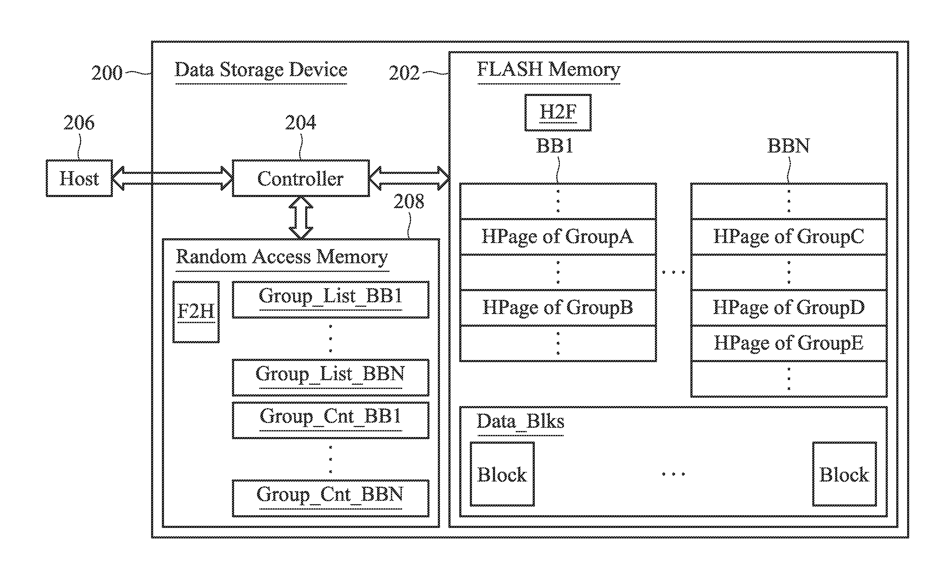
[0020]For a FLASH memory operated according to commands issued from a host, a logical-to-physical address mapping table between the host and FLASH memory is required. The logical-to-physical address mapping table should be updated onto the FLASH memory for non-volatile storage.

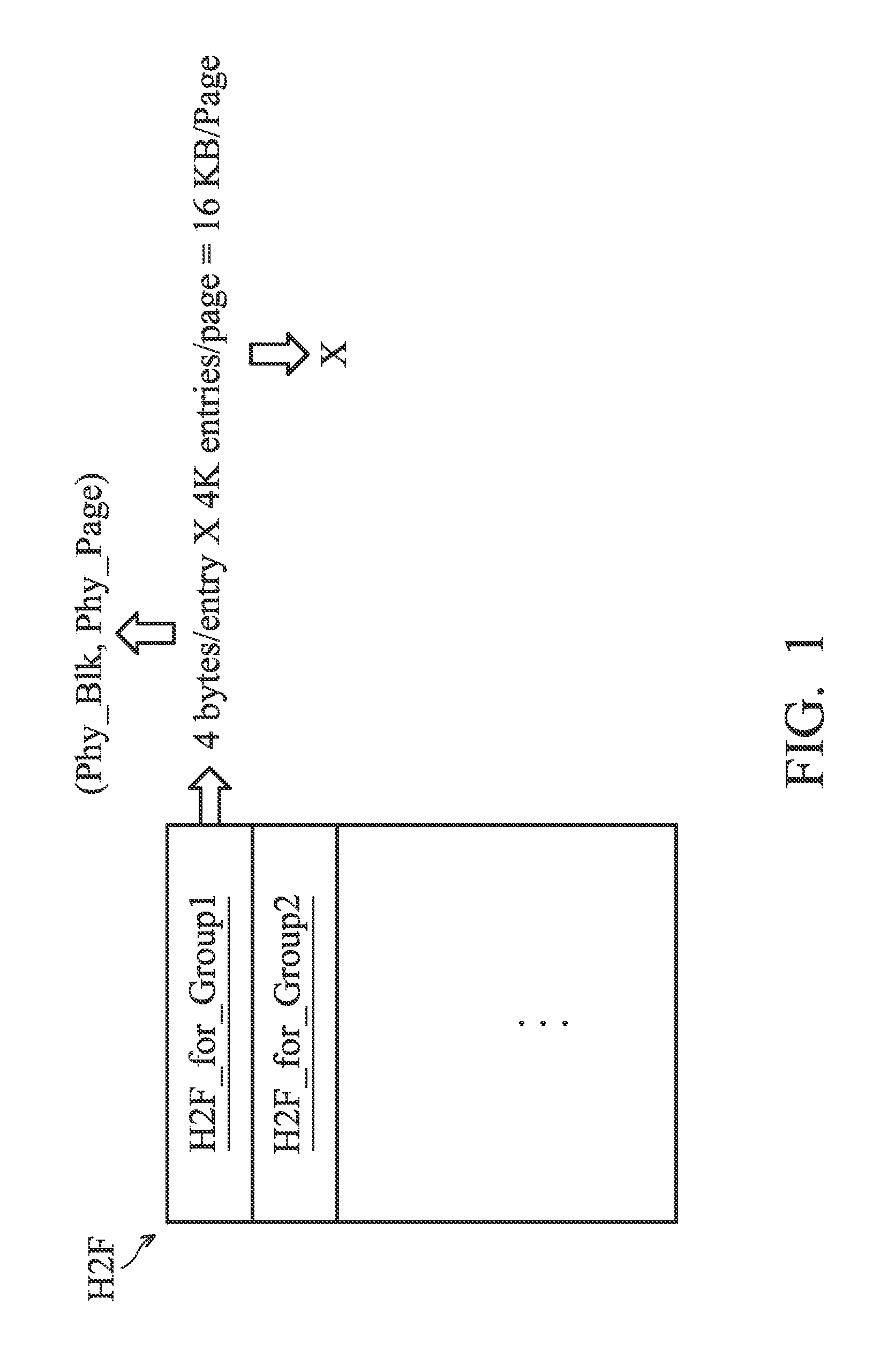
[0021]FIG. 1 shows a logical-to-physical address mapping table H2F recorded in a FLASH memory in accordance with an exemplary embodiment of the disclosure. The logical-to-physical address mapping table H2F is stored in a plurality of pages H2F_for_Group1, H2F_for_Group2 and so on. Each page of the logical-to-physical address mapping table H2F is divided into X entries for storage of the physical ...


PUM


Abstract

A mapping table H2F update technique for a FLASH memory is disclosed. In a disclosed data storage device, the controller updates a logical-to-physical address mapping table between a host and the FLASH memory in accordance with a group count of a buffer block of the FLASH memory. The group count reflects a logical address distribution of write data buffered in the buffer block and with non-updated logical-to-physical address mapping information. The higher the group count, the more dispersed the logical address distribution. In this manner, each update of the logical-to-physical address mapping table just takes a short time.

Description

CROSS REFERENCE TO RELATED APPLICATIONS[0001]This application claims the benefit of U.S. Provisional Application No. 61 / 703,443 filed Sep. 20, 2012, the entirety of which is incorporated by reference herein.BACKGROUND OF THE INVENTION[0002]1. Field of the Invention[0003]The present invention relates to data storage devices, and in particular to FLASH memory control methods.[0004]2. Description of the Related Art[0005]A Flash memory is a general non-volatile storage device that is electrically erased and programmed A NAND Flash, for example, is primarily used in memory cards, USB flash devices, solid-state drives, eMMCs (embedded MultiMediaCards), and so on.[0006]A FLASH memory may be coupled to a host as a data storage medium. Therefore, a logical-to-physical address mapping table between the host and the FLASH memory is required. The maintenance of the logical-to-physical address mapping table is an important issue.BRIEF SUMMARY OF THE INVENTION[0007]A data storage device and a FLA...

Claims


Application Information

Patent Timeline
IPC IPC(8): G06F12/02
CPCG06F12/0246
Inventor CHENG, CHANG-KAI
Owner SILICON MOTION INC (TW)
Features
  • R&D
  • Intellectual Property
  • Life Sciences
  • Materials
  • Tech Scout
  • Unparalleled Data Quality
  • Higher Quality Content
  • 60% Fewer Hallucinations
Learn More