Information processing device including memory management device managing access from processor to memory and memory management method

a technology of information processing device and memory management device, which is applied in the direction of memory adressing/allocation/relocation, program control, instruments, etc., can solve the problems of difficult control of managing bad blocks, difficult to effect optimization between operations in difference layers, and expensive drams having the same capacity

Active Publication Date: 2010-03-11
KIOXIA CORP
View PDF10 Cites 171 Cited by
  • Summary
  • Abstract
  • Description
  • Claims
  • Application Information

AI Technical Summary

Benefits of technology

[0020]An information processing device including a memory management device according to the first example of the invention comprises: an accepting section which accepts a write destination logical address and write target data from a processor, the write destination logical address indicating a write position to write the write target data into a composite memory which includes a first memory and a nonvolatile second memory; an address determining section which determines a write destination physical address corresponding to the write destination logical address so that the number of times of access to the second memory is smaller than the number of times of access to the first memory; an address management section which stores, in a storage section, address conversion data associating the write destination logical address with the write destination physical address; and a writing section which writes the write target data into a position in the composite memory indicated by the write destination physical address.

Problems solved by technology

It is difficult to effect optimization between operations in difference layers.
For example, it is difficult to realize control of managing bad block peculiar to the NAND type flash memory when the MPU makes a changeover of data of the cache memory.
However, an expensive DRAM having the same capacity as the inexpensive NAND type flash memory needs to be installed in this method.
Thus, this method is easily applied to a device having a low-capacity memory such as a mobile device, but is not easily applied to other device having greater storage capacity.

Method used


Image

  • Information processing device including memory management device managing access from processor to memory and memory management method
  • Information processing device including memory management device managing access from processor to memory and memory management method
  • Information processing device including memory management device managing access from processor to memory and memory management method

Examples


first embodiment

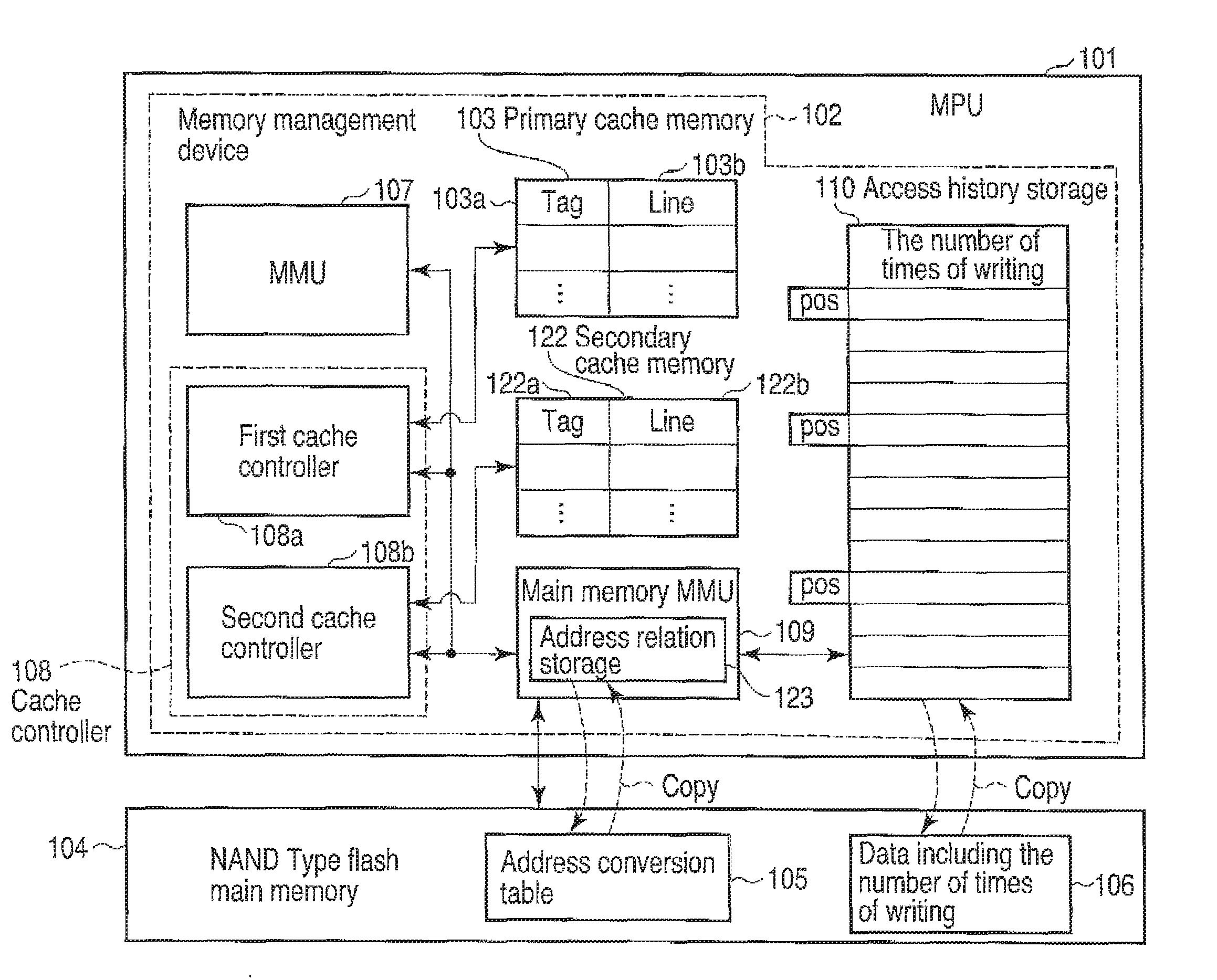
[0080]A memory management device (flat memory management device) of this embodiment is included in a MPU. The memory management device makes memory management with respect to a cache memory and a main memory. The memory management device reduces the number of memory hierarchies related to memory access, and easily realizes optimization of memory access.

[0081]In this embodiment, a nonvolatile semiconductor memory is used as the main memory. However, a composite (hybrid) main memory including a first memory and a nonvolatile second memory as described in the following ninth embodiment and after the ninth embodiment may be used as the main memory.

[0082]This embodiment relates to a memory management device, which is integrated with a MMU of MPU, a cache controller of the MPU and a main memory MMU.

[0083]FIG. 1 is a block diagram showing an example of the memory management device according to this embodiment. A main memory is a NAND type flash memory in the case described by way of exampl...

second embodiment

[0155]The second embodiment relates to a modification example of the foregoing first embodiment.

[0156]FIG. 6 is a block diagram indicating an example of a memory management device according to the second embodiment.

[0157]A MPU 111 includes a memory management device 112 according to the second embodiment. An integrated MMU 113 realizes a function of integrating the MMU 107 and the main memory MMU 109 of the first embodiment.

[0158]According to the second embodiment, each tag of the primary and secondary cache memories 103 and 122 is used for managing the cache memories 103 and 122 using a process ID and a logical address.

[0159]According to this embodiment, the integrated MMU 113 of MPU 111 as a processor executes a memory mapping management of the primary and secondary cache memories 103, 122 and the NAND type flash main memory 104. In this way, various memories are integrally managed by the integrated MMU 113.

[0160]FIG. 7 is a view indicating an example of a memory hierarchy of the ...

third embodiment

[0166]The third embodiment relates to modification examples of the memory management devices 102 and 112 according to the foregoing first and second embodiments.

[0167]FIG. 8 is a block diagram indicating an example of an memory management device 102 according to a modification example of the first embodiment.

[0168]In the foregoing first embodiment, the main memory MMU 109 accesses the NAND type flash main memory 104 based on the physical address. However, the cache controller 108 may execute access to the NAND type flash main memory 104 based on the physical address.

[0169]In this case, the main memory MMU 109 executes control of converting a logical address to a physical location. Then, the cache controller 108 accesses the NAND type flash main memory 104 based on the physical location selected by the main memory MMU 109. According to this embodiment, the cache controller 108 reads and updates the address conversion table 105 and the write number data 106 of the NAND type flash main...


PUM


Abstract

A device according to an example of the invention comprises a section which accepts a write destination logical address and write target data from a processor, the write destination logical address indicating a write position to write the write target data into a composite memory which includes a first memory and a nonvolatile second memory, a section which determines a write destination physical address corresponding to the write destination logical address so that the number of times of access to the second memory is smaller than the number of times of access to the first memory, a section which stores, in a storage section, address conversion data associating the write destination logical address with the write destination physical address, and a section which writes the write target data into a position in the composite memory indicated by the write destination physical address.

Description

CROSS-REFERENCE TO RELATED APPLICATIONS[0001]This application is based upon and claims the benefit of priority from prior Japanese Patent Applications No. 2008-231363, filed Sep. 9, 2008; and No. 2009-169371, filed Jul. 17, 2009, the entire contents of both of which are incorporated herein by reference.BACKGROUND OF THE INVENTION[0002]1. Field of the Invention[0003]The present invention relates to an information processing device including a memory management device managing an access from a processor to a memory and a memory management method.[0004]2. Description of the Related Art[0005]A conventional micro processing unit (MPU) uses a dynamic random access memory (DRAM) as a main memory (main storage). Moreover, the conventional MPU uses, for example, a flash memory as a secondary memory device. The conventional MPU and the flash memory are connected together via an I / O interface. The flash memory is treated as a file memory by the MPU.[0006]Conventionally, a management function o...

Claims


Application Information

Patent Timeline
Patent Type & Authority Applications(United States)
IPC IPC(8): G06F12/00G06F12/16G06F12/02
CPCG06F12/0246G06F12/08G06F12/0804G06F2212/205G06F2212/1036G06F2212/2022G06F2212/7201G06F12/0888G06F12/02G06F12/06
Inventor KUNIMATSU, ATSUSHINAKAI, HIROTOSAKAMOTO, HIROYUKIMAEDA, KENICHIMIYAGAWA, MASAKINOZUE, HIROSHIKAWAGOME, KAZUHIRO
Owner KIOXIA CORP
Why Eureka
Try Eureka