Unlock instant, AI-driven research and patent intelligence for your innovation.

Process of making a structure for encapsulating LED chips and the LED chips encapsulation structure

a technology of led chips and encapsulation structures, which is applied in the direction of semiconductor/solid-state device manufacturing, semiconductor devices, electrical apparatus, etc., can solve the problems of ineffective exit of thermosetting materials, suffering from the encapsulation structure of conventional led chips, and inability to effectively exi

Inactive Publication Date: 2014-04-24
CHANG WAH ELECTROMATERIALS INC +1
View PDF2 Cites 5 Cited by
  • Summary
  • Abstract
  • Description
  • Claims
  • Application Information

AI Technical Summary

Benefits of technology

This patent describes a process for making a structure that encapsulates multiple LED chips. The process involves punching a reflective substrate and an insulating substrate into layers with rows of respective through holes. A sheet-like flexible material is then mechanically roughened on both its top and bottom surfaces. The insulating material is then filled around the through holes and the rough surfaces are adhered together. The resulting structure has an airtight coating that covers the top and bottom surfaces and the solder pads and lead legs. The technical effects of this process include improved heat dissipation, improved lighting efficiency, and protection of the LED chips from damage during assembly.

Problems solved by technology

However, the conventional LED chips encapsulation structure 6 suffered a number of drawbacks.
For example, the reflective substrate 60 is made of thermosetting material which cannot effectively exiting heat generated by the LED chip 62 after a relatively long period of operation (i.e., having poor thermal conduction).
And in turn, it can damage the reflective substrate 60 and lower light being emitted.

Method used


Image

  • Process of making a structure for encapsulating LED chips and the LED chips encapsulation structure
  • Process of making a structure for encapsulating LED chips and the LED chips encapsulation structure
  • Process of making a structure for encapsulating LED chips and the LED chips encapsulation structure

Examples


Embodiment Construction

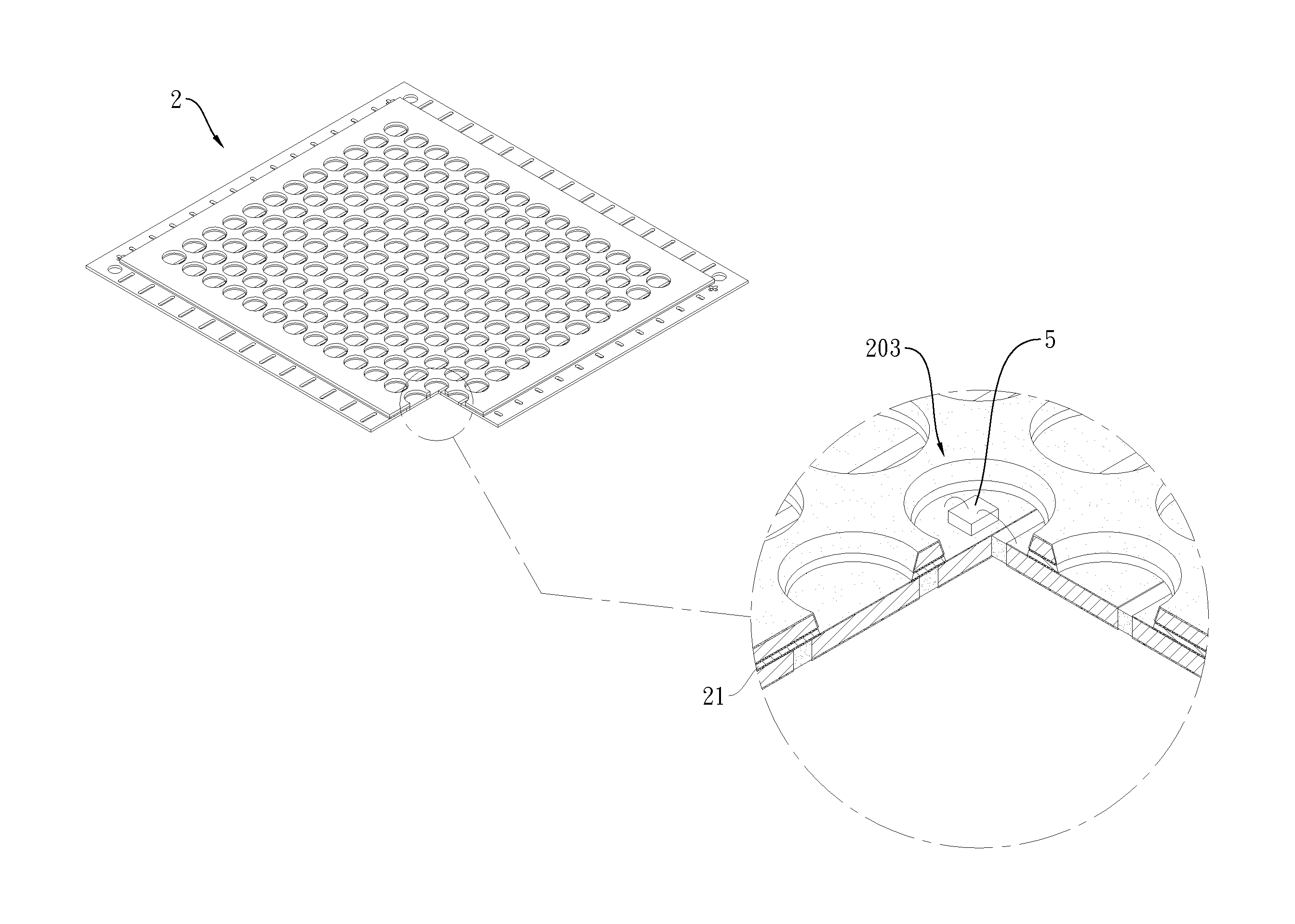
[0015]Referring to FIGS. 2 to 6, a process 1 of making a structure for encapsulating LED chips in accordance with the invention is illustrated. The process 1 comprises the following steps:

[0016]Punching step 10 is performed on a reflective substrate 200 formed of copper clad as illustrated in FIG. 2. As such, a reflective layer 20 is formed with a plurality of through holes 201 either being cylindrical or tapered downward and arranged in rows. A mechanically roughening 11 is done on a bottom of the reflective substrate 200 so as to form a rough surface 202 on the bottom of the reflective substrate 200. The rough surface 202 can increase contact area. Further, a chemically roughening 11′ is done on the rough surface 202 for forming a rough surface 202′ with increased roughness if the rough surface 202 formed by the mechanically roughening 11 is not sufficiently rough in which the chemically roughening 11′ includes steps of rubbing the rough surface 202 with a predetermined chemical s...


PUM


Abstract

A process of making a structure for encapsulating LED chips is provided with punching a reflective substrate into a reflective layer including through holes as reflective cups; punching an insulating substrate into an insulating layer including through holes, a flexible member having top and bottom formed with top and bottom layers of thermoset respectively, and top and bottom coatings formed on the top and bottom layers of thermoset respectively; punching a conductive substrate to form conductive members each having a solder pad and a lead leg; roughening bottom of the reflective layer; roughening top of the conductive substrate; filling an insulating material around the solder pads and the lead legs to form a lead frame; stacking and fastening the reflective layer, the insulating layer, and the lead frame fastened together; and electroplating the stack to form an airtight radiation emitting coating, thereby forming an LED chips encapsulation structure.

Description

BACKGROUND OF THE INVENTION[0001]1. Field of the Invention The invention relates to semiconductor device packaging and more particularly to a process of making a structure for encapsulating LED chips and the LED chips encapsulation structure.[0002]2. Description of Related Art[0003]A conventional LED chips encapsulation structure 6 is schematically illustrated in FIG. 1 and comprises a reflective substrate 60 having a coated metal thereon as a radiation emitting surface 63, a lead frame 61 formed with a bottom surface of the reflective substrate 60, a light-emitting diode (LED) chip 62 formed on the lead frame 61 in a recess of the reflective substrate 60, and two leads (not numbered) connected the LED chip 62 to anode and cathode of the lead frame 61 respectively.[0004]However, the conventional LED chips encapsulation structure 6 suffered a number of drawbacks. For example, the reflective substrate 60 is made of thermosetting material which cannot effectively exiting heat generated...

Claims


Application Information

Patent Timeline
Patent Type & Authority Applications(United States)
IPC IPC(8): H01L33/52H01L33/60
CPCH01L25/0753H01L33/60H01L33/62H01L2224/48091H01L33/52H01L2924/0002H01L2933/0033H01L2924/00014
Inventor HUANG, CHIA-NENG
Owner CHANG WAH ELECTROMATERIALS INC
Features
  • R&D
  • Intellectual Property
  • Life Sciences
  • Materials
  • Tech Scout
  • Unparalleled Data Quality
  • Higher Quality Content
  • 60% Fewer Hallucinations
Learn More