Nonvolatile Logic Circuit

a logic circuit and non-volatile technology, applied in the field of non-volatile logic circuits, can solve the problems of substantial increase of power consumption of the inverter, loss of logic state, volatile state of the cmos inverter b>10/b>,

Inactive Publication Date: 2014-06-12
SHUKH ALEXANDER MIKHAILOVICH
View PDF16 Cites 11 Cited by
  • Summary
  • Abstract
  • Description
  • Claims
  • Application Information

AI Technical Summary

Problems solved by technology

However the CMOS inverter 10 is volatile and loses its logic state when the power is off.
The opposite polarity of the voltage sources is not desirable since it leads to a substantial increase of power consumption by the inverter due to a power leakage in the transistors.

Method used


Image

  • Nonvolatile Logic Circuit
  • Nonvolatile Logic Circuit
  • Nonvolatile Logic Circuit

Examples


first embodiment

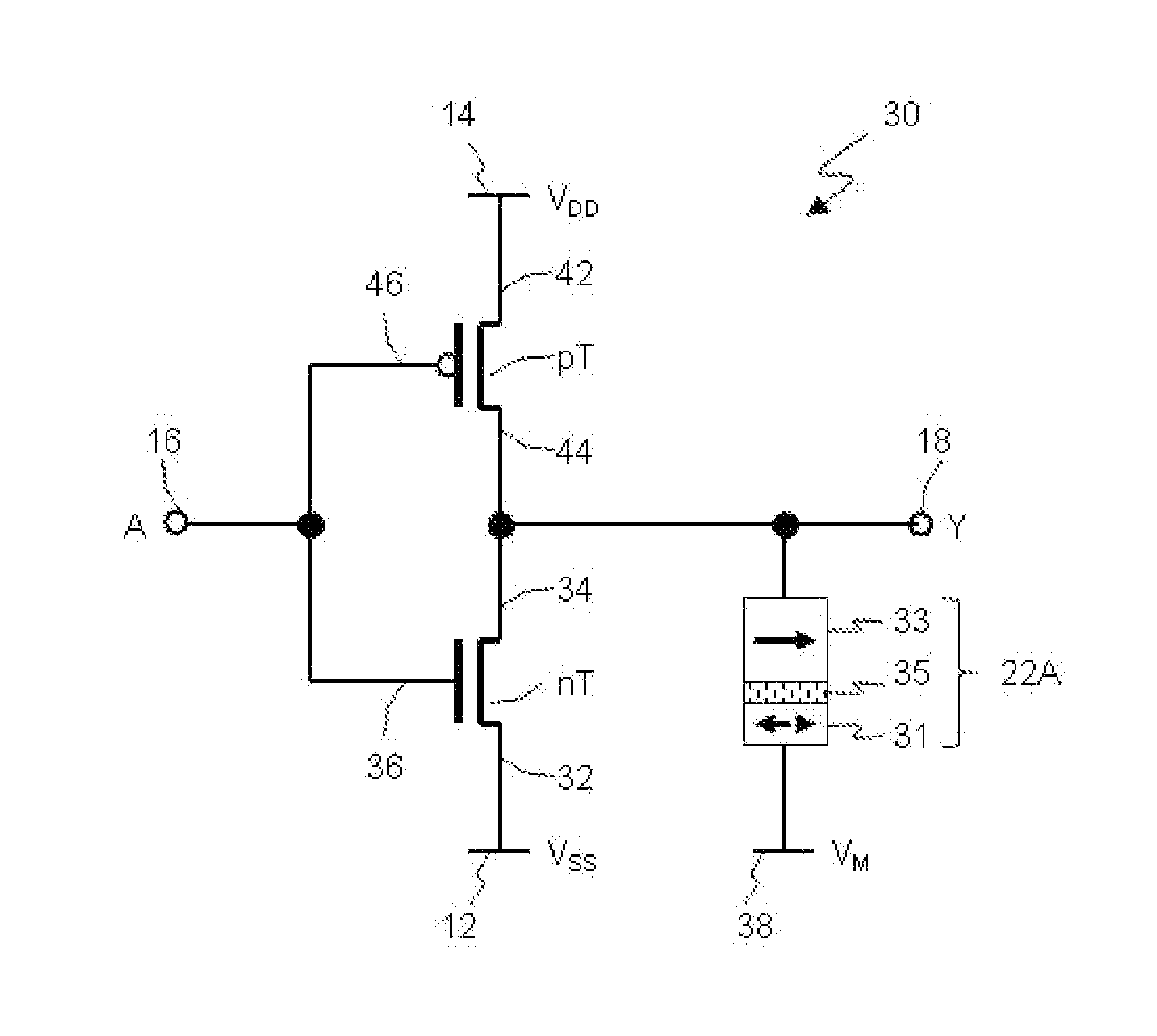
[0064]FIG. 3 illustrates a circuit diagram of a nonvolatile inverter 30 according to a The inverter 30 represents a nonvolatile logic circuit (or gate) that performs a logic function NOT. The inverter 30 comprises a n-channel MOS transistor nT and a complementary p-channel MOS transistor pT connected in series, and a magnetic tunnel junction (MTJ) 22A. A source terminal 32 of the nT transistor is connected to a low voltage source 12 (VSS). Alternatively, a source terminal 42 of the pT transistor is connected to a high voltage source 14 (VDD). Drain terminals 34 and 44 of the nT and pT transistors, respectively, are connected in common and to an output terminal 18. Gate terminals 36 and 46 of the nT and pT transistors, respectively, are connected in common and to an input terminal 16. The MTJ 22A is connected to the output terminal 18 at its first end and to an intermediate (or medium) voltage source 38 (VM) at its second end. There is a following relation between potentials of the ...

second embodiment

[0075]FIGS. 6A and 6B show an nonvolatile logic circuit 60 performing a buffer function according to a Similar to the nonvolatile inverter 30 disclosed above (FIG. 3), the nonvolatile buffer 60 utilizes CMOS technology with one n-channel and one p-channel transistor nT and pT, respectively, connected in series. A source terminal 32 of the transistor nT is connected to a low voltage source 32 (VSS), and a source terminal 42 of the pT transistor is connected to a high voltage source 14 (VDD). Gate terminals 36 and 46 of the transistors nT and pT, respectively, are connected in common and to an input terminal 16. Similarly, drain terminals 34 and 44 of the transistors nT and pT, respectively, are connected in common and to an output terminal 18. A MTJ 22B is connected to the output terminal 18 at its first end and to an intermediate voltage source 38 (VM) at its second end. More specifically, a pinned layer 33 of the MTJ 22B is disposed adjacent the voltage source 38, and a free layer...

fourth embodiment

[0086]FIG. 9 shows a circuit diagram of a 2-input nonvolatile logic circuit 90 according to a The logic circuit 90 performs a logic function AND. The circuit 90 has a similar circuit diagram to that of the nonvolatile logic circuit 80 shown in FIG. 8 but comprises a MTJ 22B, wherein the free layer 31 is disposed adjacent the output terminal 18 and the pinned layer 33 is disposed adjacent the intermediate voltage source 38. A reversed position of the free 31 layer relatively to the output terminal 18 in the logic circuit 90 compared to that in the logic circuit 80 results in an reversed polarity of the output signal Y when similar combinations of the signals A and B appear at the input terminals 16A and 16B. A truth table of the nonvolatile logic circuit 90 performing AND function is given in Table 4.


PUM


Abstract

One embodiment of a nonvolatile logic circuit includes a logic circuit comprising a first source terminal, a second source terminal, at least one input terminal, and an output terminal to temporarily store a logic state with a power dependent status, a high voltage source coupled to the first source terminal, a low voltage source coupled to the second source terminal, an intermediate voltage source comprising an electrical potential higher than that of the low voltage source but lower than that of the high voltage source, and a nonvolatile reversible resistance element coupled to the output terminal at a first end and to the intermediate voltage source at a second end. The nonvolatile reversible resistance element preserves the logic state of the logic circuit which is controlled by an input signal applied to the at least one input terminal. Other embodiment are described and shown.

Description

CROSS-REFERENCE TO RELATED APPLICATIONS[0001]This application is a continuation-in-part of U.S. patent application Ser. No. 13 / 283,465, filed on Oct. 27, 2011 and claims the benefit of U.S. provisional patent application No. 61 / 408,550, filed on Oct. 29, 2010 by the present inventor.FEDERALLY SPONSORED RESEARCH[0002]Not ApplicableSEQUENCE LISTING OR PROGRAM[0003]Not ApplicableRELEVANT PRIOR ART[0004]U.S. Pat. No. 3,356,858, Dec. 5, 1967—Wanlass.[0005]U.S. Pat. No. 7,339,818, Mar. 4, 2008—Katti et al.[0006]U.S. Pat. No. 7,894,248, Feb. 22, 2011—Yu et al.[0007]U.S. Pat. No. 8,004,882, Aug. 23, 2011—Katti et al.[0008]U.S. Patent Application Publication No. 2010 / 0039136, Feb. 18, 2010—Chua-Eoan et al.BACKGROUND[0009]A logic gate is an arrangement of electronically controlled switches used to proceed calculations in Boolean algebra. Logic gates can be constructed from relays, diodes, transistors and other elements. The logic gates constructed from the metal-oxide-semiconductor (MOS) tran...

Claims


Application Information

Patent Timeline
Patent Type & Authority Applications(United States)
IPC IPC(8): H03K19/173
CPCH03K19/173H03K19/168G11C13/0002H03K19/16
Inventor SHUKH, ALEXANDER MIKHAILOVICH
Owner SHUKH ALEXANDER MIKHAILOVICH
Why Eureka
Try Eureka