
Method for polishing silicon wafer and polishing agent

a technology of silicon wafers and polishing agents, which is applied in the direction of lapping machines, manufacturing tools, chemistry apparatuses and processes, etc., can solve the problems of more polishing damage or the like in the wafer surface, and the diameter increases, and achieves accurate polishing time, high polishing rate, and constant polishing rate

Inactive Publication Date: 2014-06-12
SHIN-ETSU HANDOTAI CO LTD
View PDF2 Cites 7 Cited by
  • Summary
  • Abstract
  • Description
  • Claims
  • Application Information

AI Technical Summary

Benefits of technology

The present invention provides a method for polishing silicon wafers by adjusting the concentration of silicate ions in the polishing agent. This method maintains a high polishing rate and a constant polishing rate among polishing batches, allowing for accurate polishing time and control of the polishing stock removal or finishing thickness. Additionally, this method suppresses variation in the polishing rate over a long period of time, allowing for a longer target life of the polishing agent.

Problems solved by technology

However, the larger the particle diameter becomes, the more polishing damage or the like occurs in the wafer surface.

Method used


Image

  • Method for polishing silicon wafer and polishing agent
  • Method for polishing silicon wafer and polishing agent
  • Method for polishing silicon wafer and polishing agent

Examples


examples

[0071]Hereinafter, the present invention will be described more specifically with an example and a comparative example of the present invention, but the present invention is not limited to these examples.

example

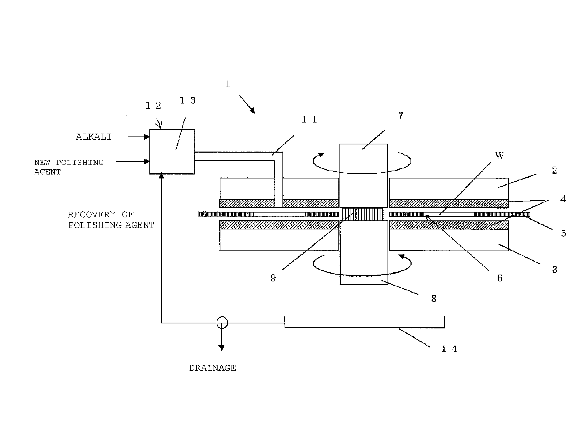
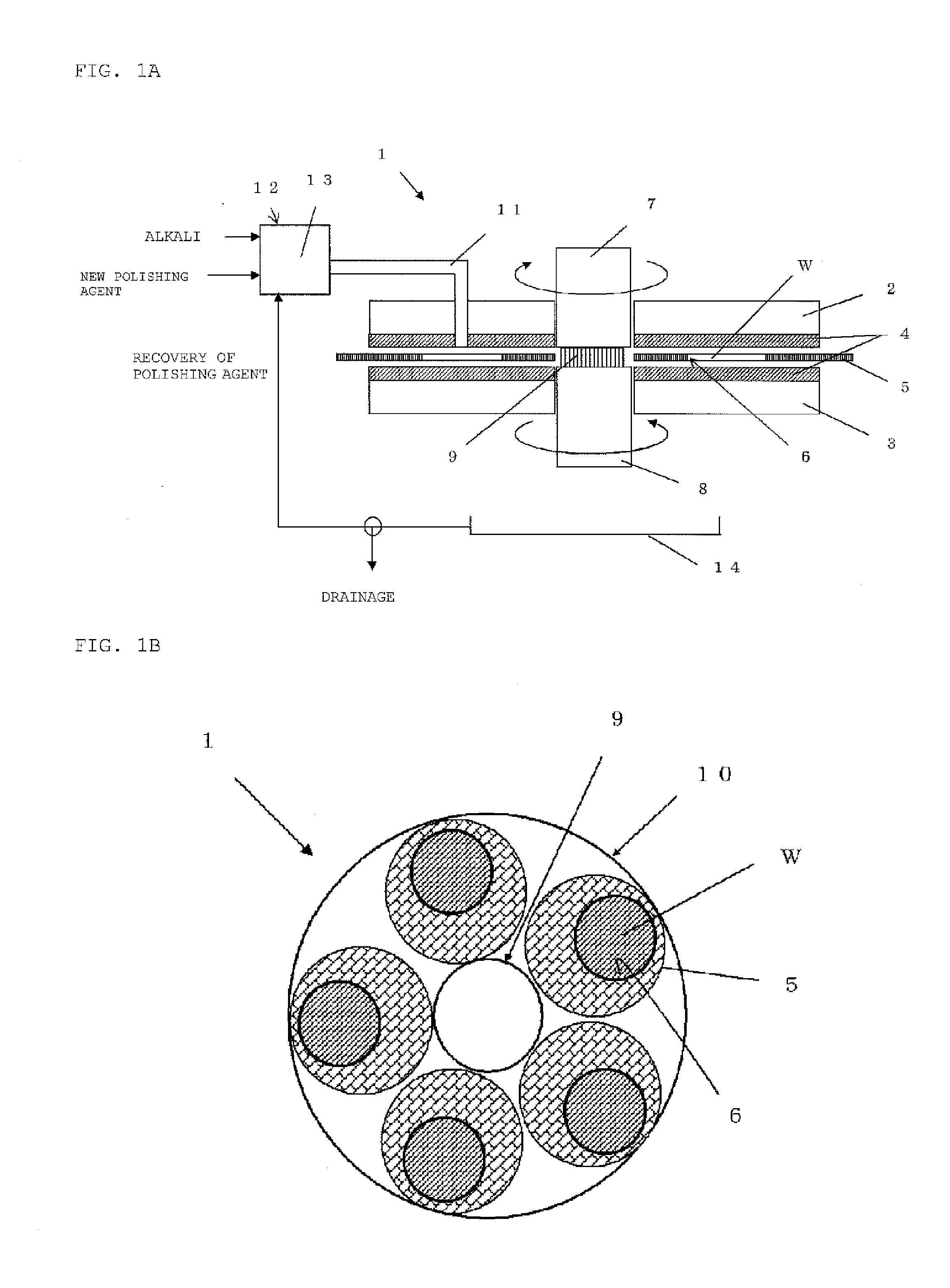
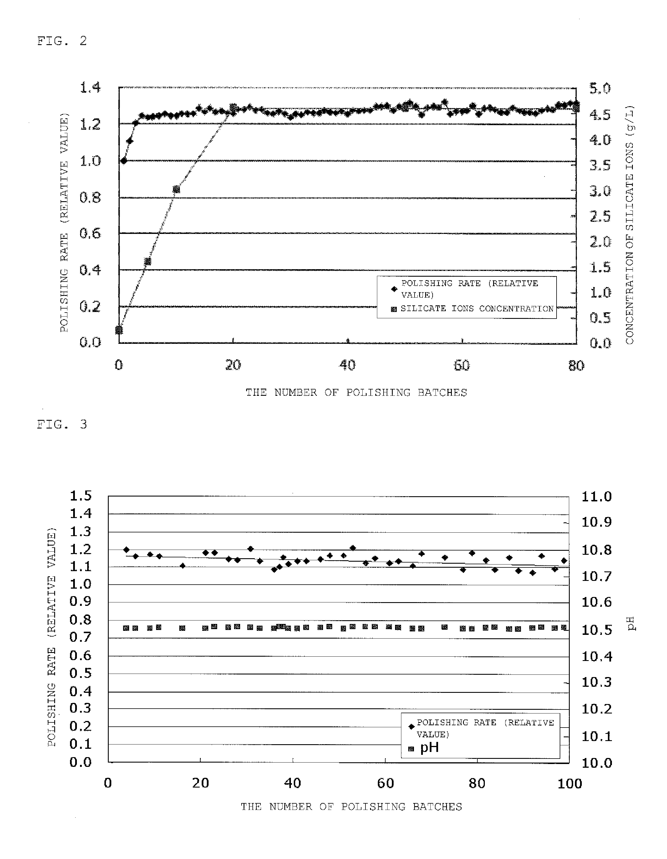
[0072]By using the double-side polishing apparatus capable of polishing five silicon wafers at the same time, as depicted in FIG. 1, polishing of silicon wafers with a diameter of 300 mm was repeated in a batch manner with the concentration of silicate ions in the polishing agent being adjusted to be 4.6 g / L, according to the method for polishing a silicon wafer of the present invention. The number of wafers to be polished per batch was five. Etched silicon wafers having a thickness of about 793±2 μm were polished under a polishing pressure of 200 g / cm2 for such a polishing time that the thickness of the wafers was reduced to 777 μm, i.e., the stock removal became about 16 μm. The polishing stock removal was examined by measuring the thickness of the polished silicon wafers, and the polishing rate was calculated from the polishing stock removal and the polishing time and evaluated.

[0073]First, the polishing agent of the present invention was created in the following manner.

[0074]Abo...


PUM


Abstract

The present invention is directed to a method for polishing a silicon wafer, the method comprising: polishing the silicon wafer by bringing the silicon wafer into sliding contact with a polishing pad attached to a turn table while supplying a polishing agent stored in a tank to the polishing pad; and circulating the polishing agent to recover the supplied polishing agent in the tank, wherein the silicon wafer is polished while adjusting a concentration of silicate ions contained in the polishing agent in the tank to be within a predetermined range. The present invention provides a polishing agent having a high polishing rate that enables the polishing rate to be kept constant among polishing batches, and a method for polishing a silicon wafer accurately with a target polishing stock removal or a target finishing thickness by using the polishing agent.

Description

TECHNICAL FIELD[0001]The present invention relates to a method for polishing a silicon wafer by bringing the silicon wafer into sliding contact with a polishing pad while supplying a polishing agent, and to the polishing agent.BACKGROUND ART[0002]In general, a method for producing a silicon wafer includes a slicing process of slicing a silicon ingot to obtain a thin disk-shaped wafer, a chamfering process of chamfering the outer region of the wafer obtained by the slicing process to prevent a fracture and a chip in the wafer, a lapping process of flattening the chamfered wafer, an etching process of removing mechanical damage remaining in the chamfered and lapped wafer, a polishing (polishing) process of mirror-polishing the front surface of the etched wafer, and a cleaning process of cleaning the polished wafer to remove a polishing agent and foreign substances attached to the wafer.[0003]Those described above are only main processes, and a heat treatment process, a surface grindin...

Claims


Application Information

Patent Timeline
IPC IPC(8): H01L21/02C09G1/02
CPCC09G1/02H01L21/02024B24B37/005B24B37/044B24B37/08
Inventor OBA, SHIGERUKAWAMATA, TAKAO
Owner SHIN-ETSU HANDOTAI CO LTD
Learn More