Method of manufacturing semiconductor device and method of testing the same
- Summary
- Abstract
- Description
- Claims
- Application Information
AI Technical Summary
Benefits of technology
Problems solved by technology
Method used
Image

Examples
Example
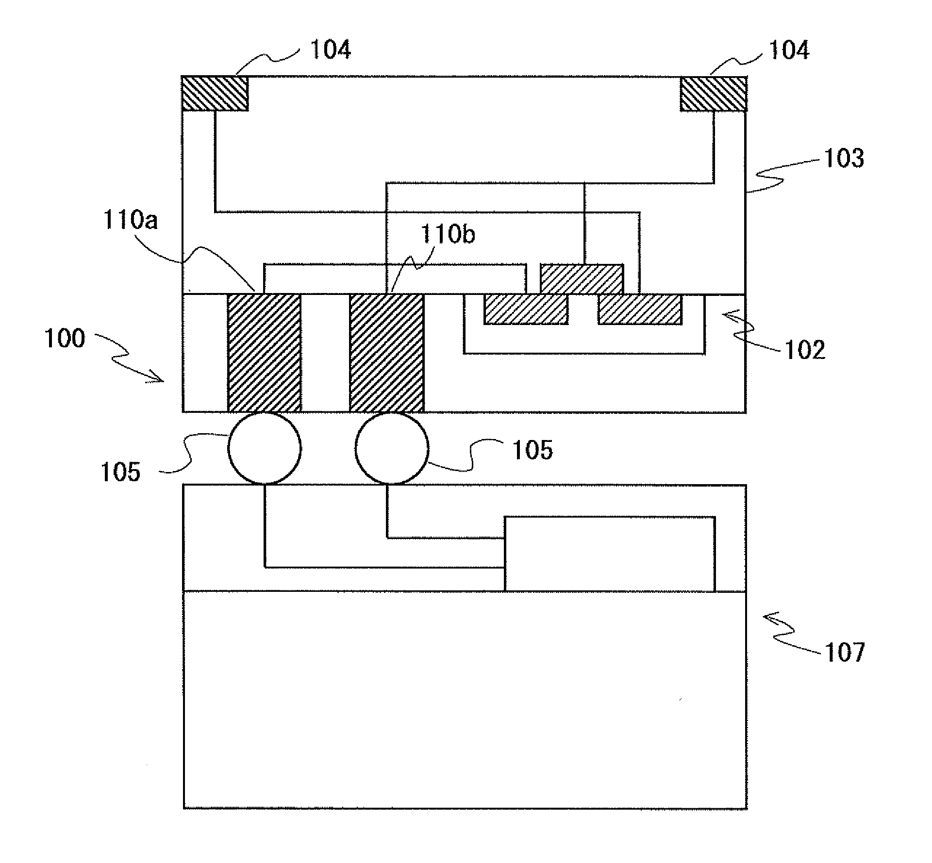
[0028]In a manufacturing process of a semiconductor device, a plurality of semiconductor chips having TSVs formed therein are integrated to form a semiconductor device. This exemplary embodiment makes it possible to test continuity of the TSVs in a state of the semiconductor chip.
[0029]Hereinafter, the exemplary embodiment of the present invention shall be explained with reference to the drawings.
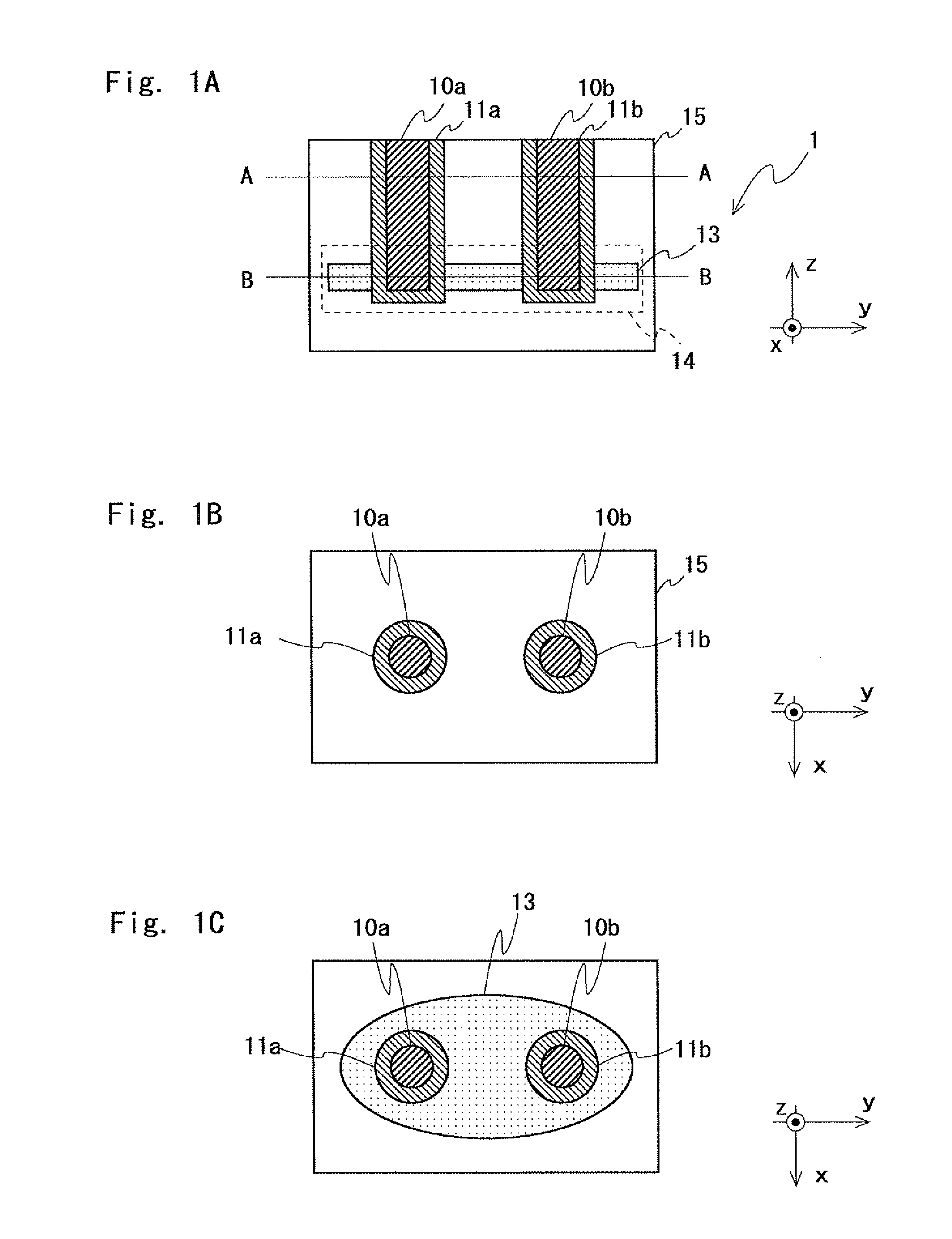
[0030]FIGS. 1A to 1C are diagrams showing a semiconductor chip 1 that is being manufactured. FIG. 1A shows a cross-section along a z axis direction of the semiconductor chip 1. Note that in the following explanation of cross-sections, hatching of silicon substrate cross-sections shall be omitted.
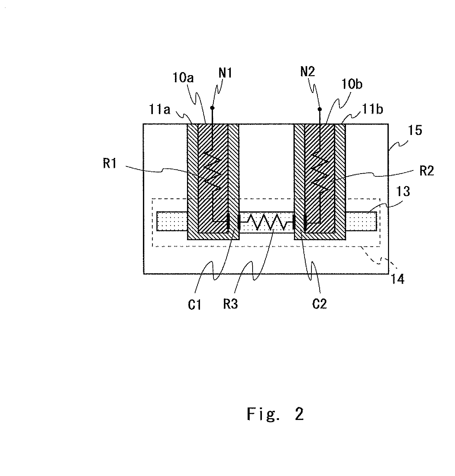
[0031]In the semiconductor chip 1, a TSV 10a covered with an insulating film 11a, a TSV 10b covered with an insulating film 11b, and a high concentration impurity region 13 are formed in a silicon substrate 15.
[0032]FIG. 1B is a diagram showing a cross-section taken along the line A-A of the semicon...
PUM
 Abstract
Description
Claims
Application Information
 - R&D Engineer
- R&D Manager
- IP Professional
- Industry Leading Data Capabilities
- Powerful AI technology
- Patent DNA Extraction
Browse by: Latest US Patents, China's latest patents, Technical Efficacy Thesaurus, Application Domain, Technology Topic.
© 2024 PatSnap. All rights reserved.Legal|Privacy policy|Modern Slavery Act Transparency Statement|Sitemap