Semiconductor memory device

Inactive Publication Date: 2002-09-19
KK TOSHIBA +1
View PDF0 Cites 160 Cited by
  • Summary
  • Abstract
  • Description
  • Claims
  • Application Information

AI Technical Summary

Benefits of technology

0007] It is therefore an object of the present invention to provide a semiconductor memory device

Problems solved by technology

However, practical use is not easy since there are a technical difficulty that the transistor has to be a vertical type, a problem that electric interference

Method used


Image

  • Semiconductor memory device
  • Semiconductor memory device
  • Semiconductor memory device

Examples


first embodiment

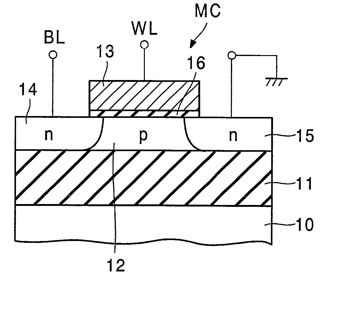
[0136] FIG. 19A shows the structure of a memory cell MC according to a first embodiment of the present invention corresponding to FIG. 1. The basic structure is the same as in FIG. 1, and FIG. 19A is different from FIG. 1 in that a second gate 20 which capacitively couples with the silicon layer 12 while facing it with a gate insulating film 19 therebetween is buried in the oxide film 11 separately from the first gate 13 to control the channel, and in that such a high concentration p.sup.+-type layer 21 that the channel inversion layer is not formed is formed on a surface on the second gate 20 side of the silicon layer 12. That is, the p.sup.+-type layer 21 is formed in the silicon layer 12, and conductive type of the p.sup.+-type layer 21 is the same as that of the silicon layer 12 and impurity concentration of the p.sup.+-type layer 21 is higher than that of the silicon layer 12. Since the p.sup.+-type layer 21 exits, even when a positive potential is applied to the first gate 13 ...

second embodiment

[0161] FIG. 20 shows the structure of a memory cell MC according to a second embodiment. Differently from the embodiment in FIG. 19A, in this embodiment, the second gate 20 is disposed as a common gate (back plate) so as to cover the entire cell array region without being patterned as lines. Namely, the second gate 20 is provided for all the MIS transistors in the memory cell array. According to such a structure, the alignment of the second gate 20 with the first gate 13 becomes unnecessary, and the manufacturing process is simplified.

[0162] In such a structure, the second gate 20 is fixed, for example, at a potential equal to or lower than a source potential, and the same operation as explained in the preceding basic memory cell is performed. Also in this case, by increasing the amplitude of the first gate 13 (word line WL), a signal difference between the "0" and "1" data can be increased. Namely, when the second gate 20 is capacitively coupled to the channel body at a fixed poten...

third embodiment

[0163] FIG. 21 shows the layout of a memory cell array according to a third embodiment, and FIG. 22 shows its section taken along the line A-A'. The SOI substrate is used for making a transistor with a floating channel body in the embodiments heretofore, while, in this embodiment, a memory cell is composed of a vertical MIS transistor with a floating channel body by using a so-called SGT (Surrounding GATE Transistor) structure.

[0164] In the silicon substrate 10, trenches running lengthwise and crosswise are formed by RIE, and P-type pillar silicon portions 30 are arranged therein. The fist gate 13 and the second gate 20 are formed to face each other on both side faces of each of the pillar silicon portions 30. The first gates 13 and the second gates 20 are buried alternately between the pillar silicon portions 30 in the section in FIG. 22. The first gates 13 are formed isolatedly as independent gate electrodes relative to the adjacent pillar silicon portions 30 between the adjacent ...


PUM


Abstract

Each of MIS transistors of a semiconductor memory device has a semiconductor layer (12); a source region (15) formed in the semiconductor layer; a drain region (14) formed apart from the source region in the semiconductor layer, the semiconductor layer between the source region and the drain region serving as a channel body in a floating state; a first gate (13) which forms a channel in the channel body; a second gate (20) formed so as to control a potential of the channel body by a capacitive coupling; and a high concentration region (21) formed in the channel body on the second gate side, impurity concentration of the high concentration region being higher than that of the channel body.

Description

CROSS REFERENCE TO RELATED APPLICATION[0001] This application claims the benefit of priority under 35 U.S.C. .sctn.119 to Japanese Patent Application No. 2001-74236 filed on Mar. 15, 2001, the entire contents of which are incorporated by reference herein.BACKGROUND OF THE INVENTION[0002] 1. Field of the Invention[0003] The present invention relates to a semiconductor memory device which dynamically stores data with using a channel body of a transistor as a storage node.[0004] 2. Related Background Art[0005] In a related DRAM, a memory cell is composed of an MOS transistor and a capacitor. The scale-down of the DRAM has been remarkably advanced by the adoption of a trench capacitor structure and a stacked capacitor structure. At present, the cell size of a unit memory cell is scaled down to an area of 2 F.times.4 F=8 F.sup.2, where F is a minimum feature size. Namely, the minimum feature size F decreases with the advance of generation, and when the cell size is generally taken to be ...

Claims


Application Information

Patent Timeline
IPC IPC(8): H01L27/108H01L27/12
CPCG11C11/404G11C2211/4016H01L27/108H01L27/10802H01L27/10823H01L27/10841H01L27/1203H01L29/7841H10B12/20H10B12/34H10B12/395H10B12/00
Inventor HORIGUCHI, FUMIOOHSAWA, TAKASHIIWATA, YOSHIHISAYAMADA, TAKASHI
Owner KK TOSHIBA
Why Eureka
Try Eureka