

Phosphor film, and light emitting device and system using the same
a technology of light emitting devices and phosphor films, which is applied in the direction of semiconductor devices, electrical devices, chemistry apparatuses and processes, etc., can solve the problems of light generated by light emitting elements that may be lost, and achieve the effect of improving the light extraction ra
- Summary
- Abstract
- Description
- Claims
- Application Information
AI Technical Summary
Benefits of technology
Problems solved by technology
Method used
Image

Examples
first embodiment
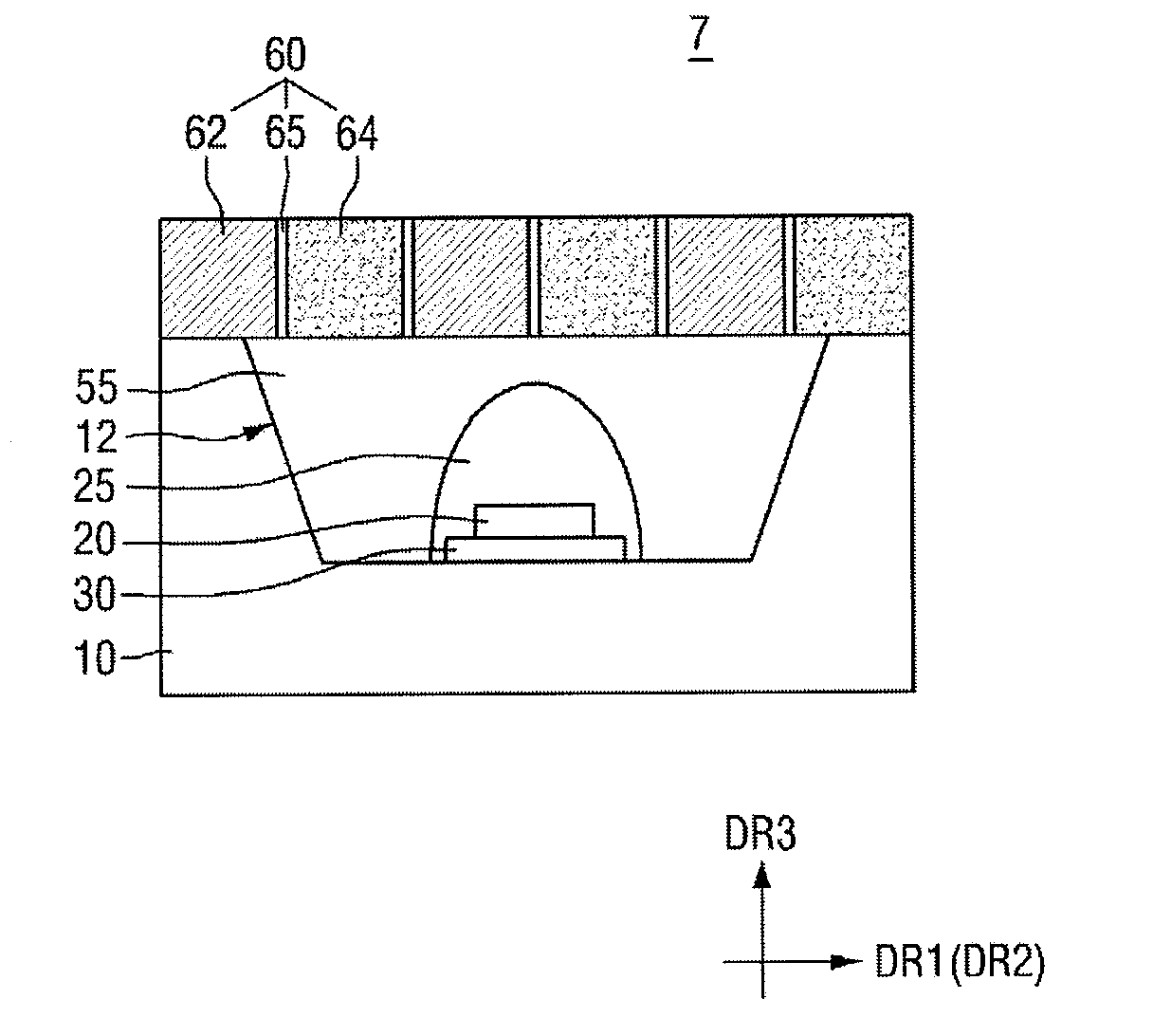
[0035]FIG. 1 is a diagram for explaining a phosphor film according to the present invention.
[0036]Referring to FIG. 1, a phosphor film 60 according to the first embodiment of the present invention includes one or more first quantum dot phosphor layers 62, one or more second quantum dot phosphor layers 64 and an adhesive layer 65.
[0037]The first quantum dot phosphor layers 62 may be formed to be spaced apart from each other. The first quantum dot phosphor layers 62 include resin and first quantum dot phosphors. That is, the first quantum dot phosphor layers 62 may include resin and first quantum dot phosphors dispersed in the resin. The resin in which the first quantum dot phosphors are dispersed may include, for example, epoxy resin, silicone resin, rigid silicone resin, modified silicone resin, urethane resin, oxetane resin, acrylic resin, polycarbonate resin, polyimide resin, or the like, but it is not limited thereto. That is, the resin may be any material capable of stably dispe...
fourth embodiment
[0063]FIG. 4 is a diagram for explaining a phosphor film according to the present invention.
[0064]Referring to FIG. 4, a phosphor film 60 according to the fourth embodiment of the present invention includes one or more first quantum dot phosphor layers 62, one or more second quantum dot phosphor layers 64, one or more third quantum dot phosphor layers 66, and an adhesive layer 65.
[0065]The first quantum dot phosphors, the second quantum dot phosphors and the third quantum dot phosphors respectively included in the first quantum dot phosphor layers 62, the second quantum dot phosphor layers 64 and the third quantum dot phosphor layers 66 may generate light of different wavelengths.
[0066]In the phosphor film according to the fourth embodiment of the present invention, the first quantum dot phosphor layers 62, the second quantum dot phosphor layers 64 and the third quantum dot phosphor layers 66 may be arranged in a mesh shape. The adhesive layer 65 may be formed on the circumstance of...
fifth embodiment
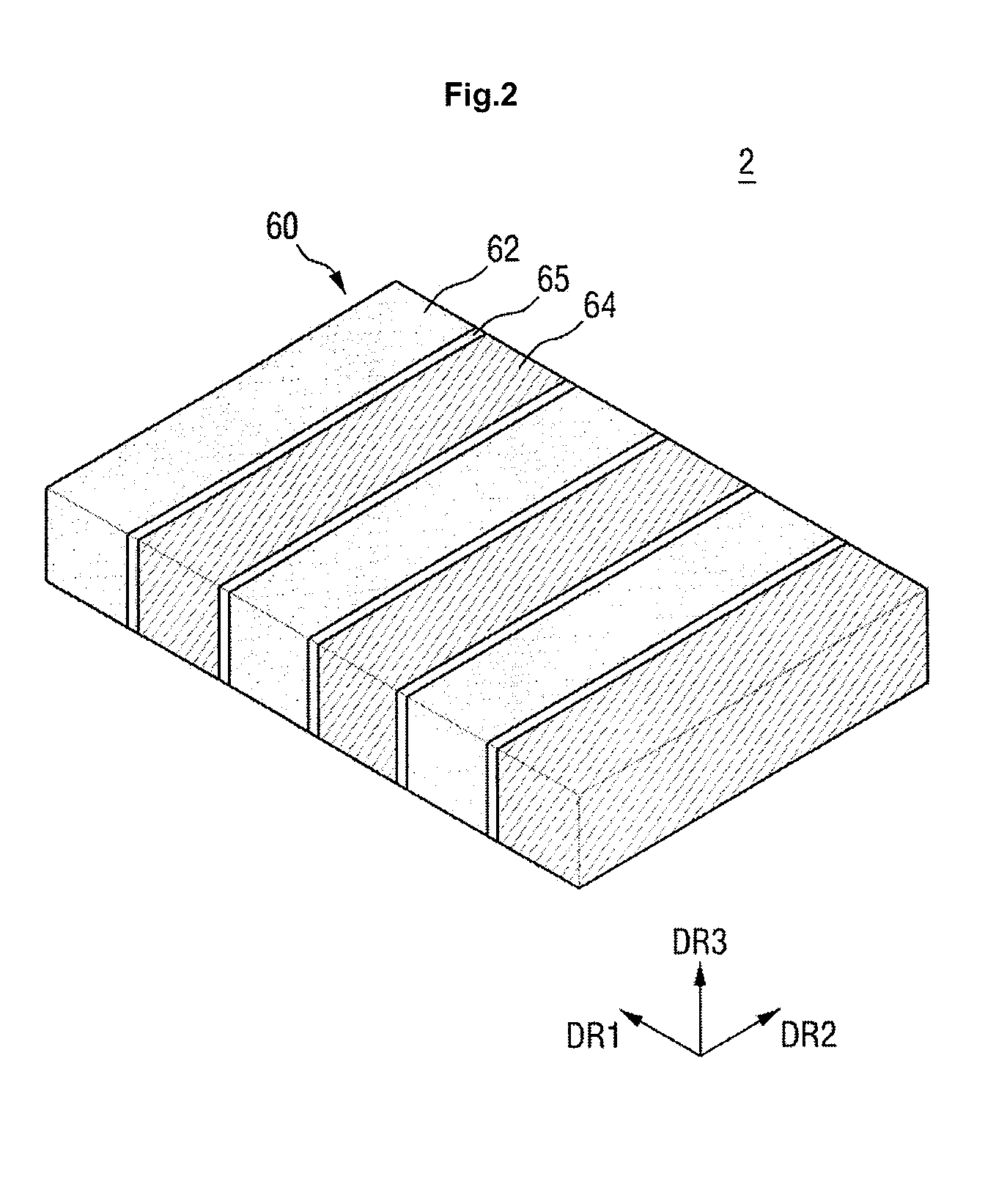
[0068]FIG. 5 is a diagram for explaining a phosphor film according to the present invention.
[0069]Referring to FIG. 5, a phosphor film 60 according to the fifth embodiment of the present invention includes first quantum dot phosphor layers 62, second quantum dot phosphor layers 64 and third quantum dot phosphor layers 66, which have a linear shape and are formed alternately.
[0070]FIG. 6 is a cross-sectional view for explaining a light emitting device 6 according to a first embodiment of the present invention. For simplicity of description, only main parts are simplified or emphasized in FIG. 6.
[0071]Referring to FIG. 6, the light emitting device 6 according to the first embodiment of the present invention may include a package body 10, a light emitting element 20, a submount 30, a resin layer 50 and a phosphor film 60.
[0072]The light emitting element 20 may be disposed on the package body 10. Specifically, the package body 10 may include a slot 12 therein, and the light emitting ele...
PUM
 Abstract
Description
Claims
Application Information