
Assembling and Handling Edge Interconnect Packaging System

Active Publication Date: 2014-09-18
INDIANA INTEGRATED CIRCUITS
View PDF8 Cites 6 Cited by
  • Summary
  • Abstract
  • Description
  • Claims
  • Application Information

AI Technical Summary

Benefits of technology

The patent describes how two sets of parts can be joined together to keep them from touching each other. This helps to maintain the space between them.

Problems solved by technology

For example, existing methods are incapable of the precision alignment required to connect multiple edge-based contact points.
Further, existing methods are inadequate at reliably forming functional mechanical and electrical connections directly between adjacent microchips.

Method used


Image

  • Assembling and Handling Edge Interconnect Packaging System
  • Assembling and Handling Edge Interconnect Packaging System
  • Assembling and Handling Edge Interconnect Packaging System

Examples


Embodiment Construction

[0031]It is advantageous to define several terms before describing particular embodiments. It should be appreciated that the following definitions are used throughout this application.

DEFINITIONS

[0032]Where the definition of terms departs from the commonly used meaning of the term, the definitions provided below are intended, unless specifically indicated otherwise.

[0033]For the purposes of the present description, the term “direct electrical connection” refers to the direct contact between interconnect nodules or between an interconnect nodule and an electrical contact so that electrical conduction current may pass between them.

[0034]For the purposes of the present description, the term “electronic device” refers to electronic circuitry and any device that includes electronic circuitry. Examples of electronic devices include, but are not limited to, microchips, package systems, transistors, printed circuit boards (PCBs), amplifiers, sensors, inductors, capacitors, electrical connec...


PUM

PropertyMeasurementUnit
Electrical conductoraaaaaaaaaa

Abstract

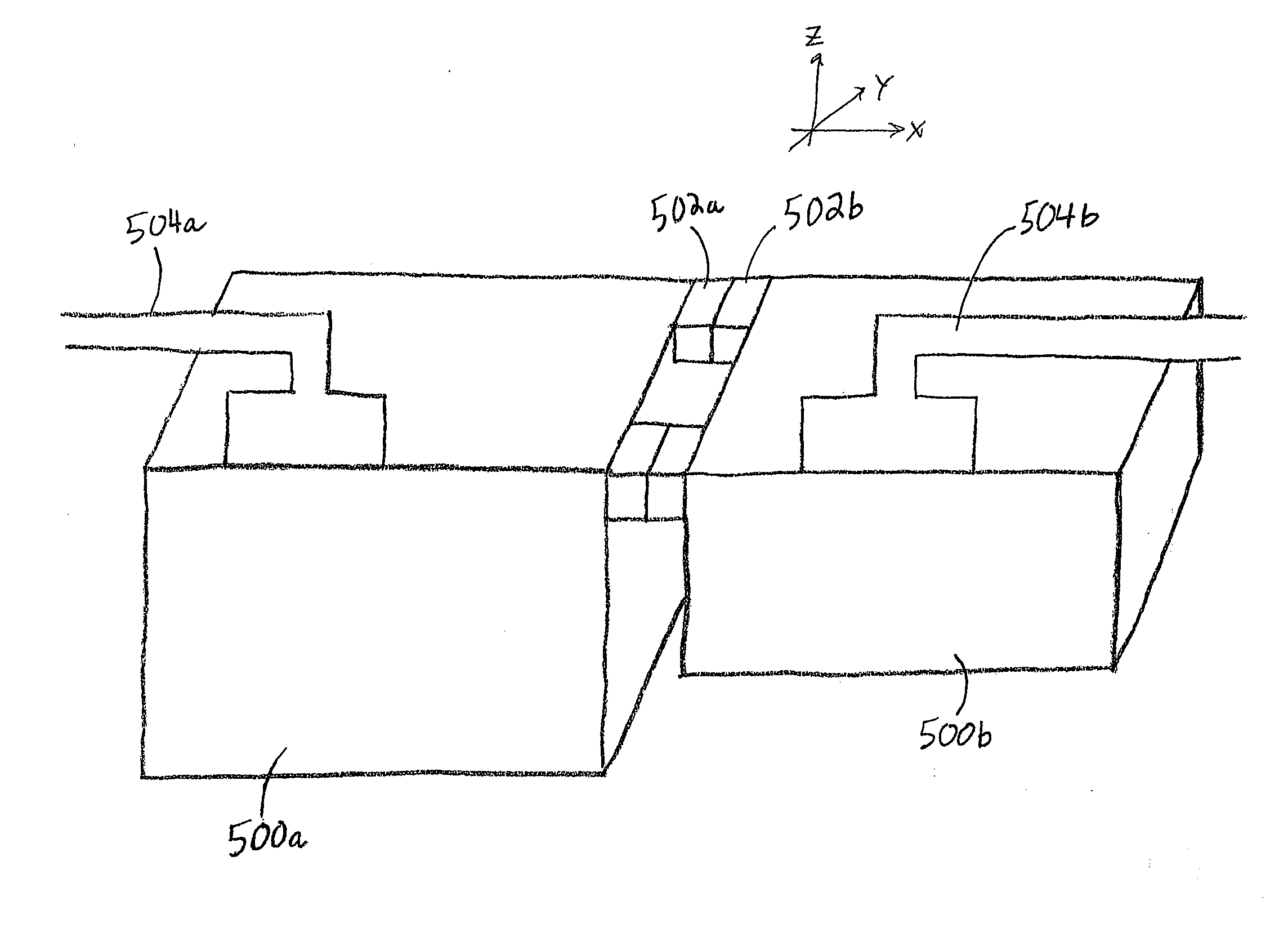
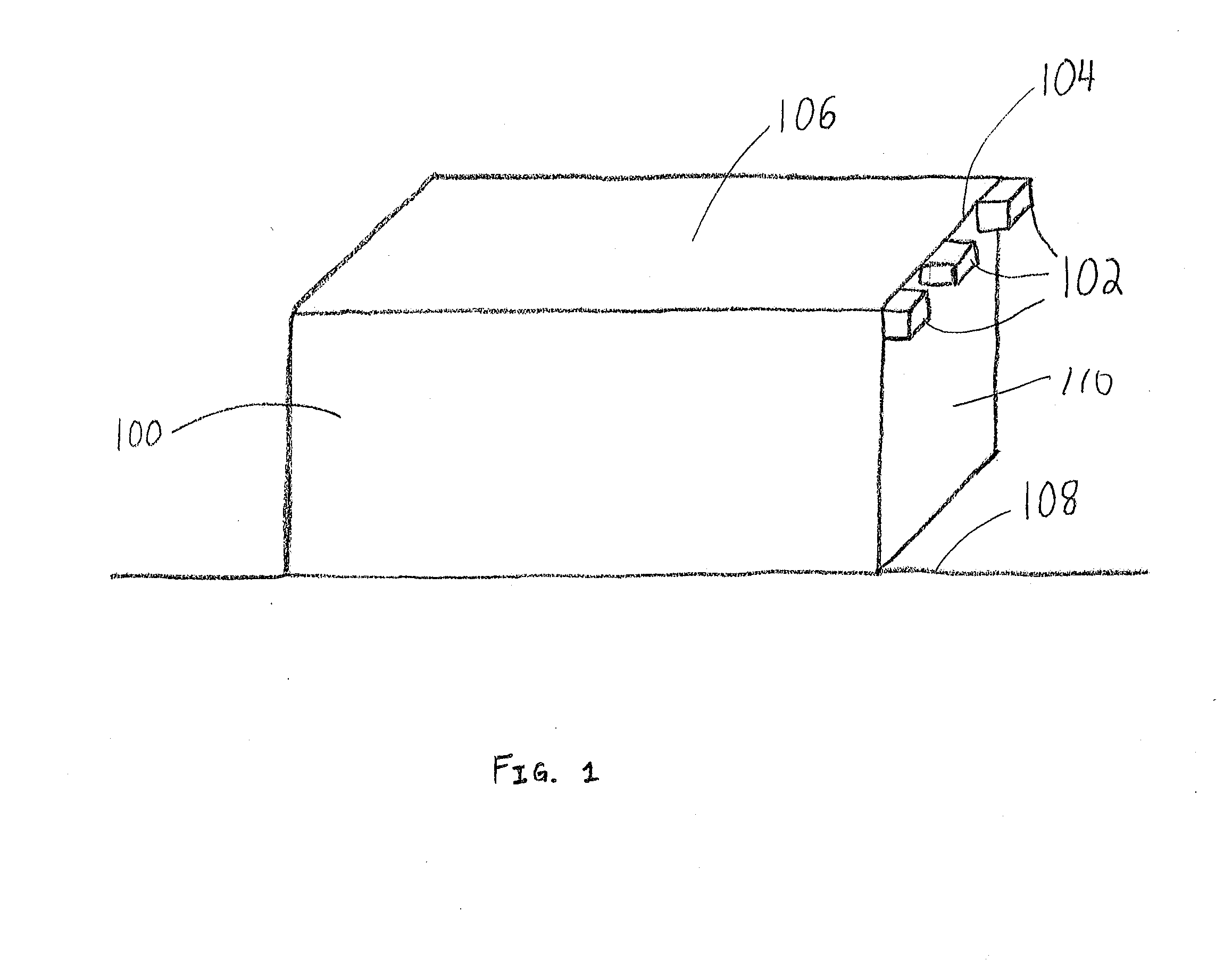
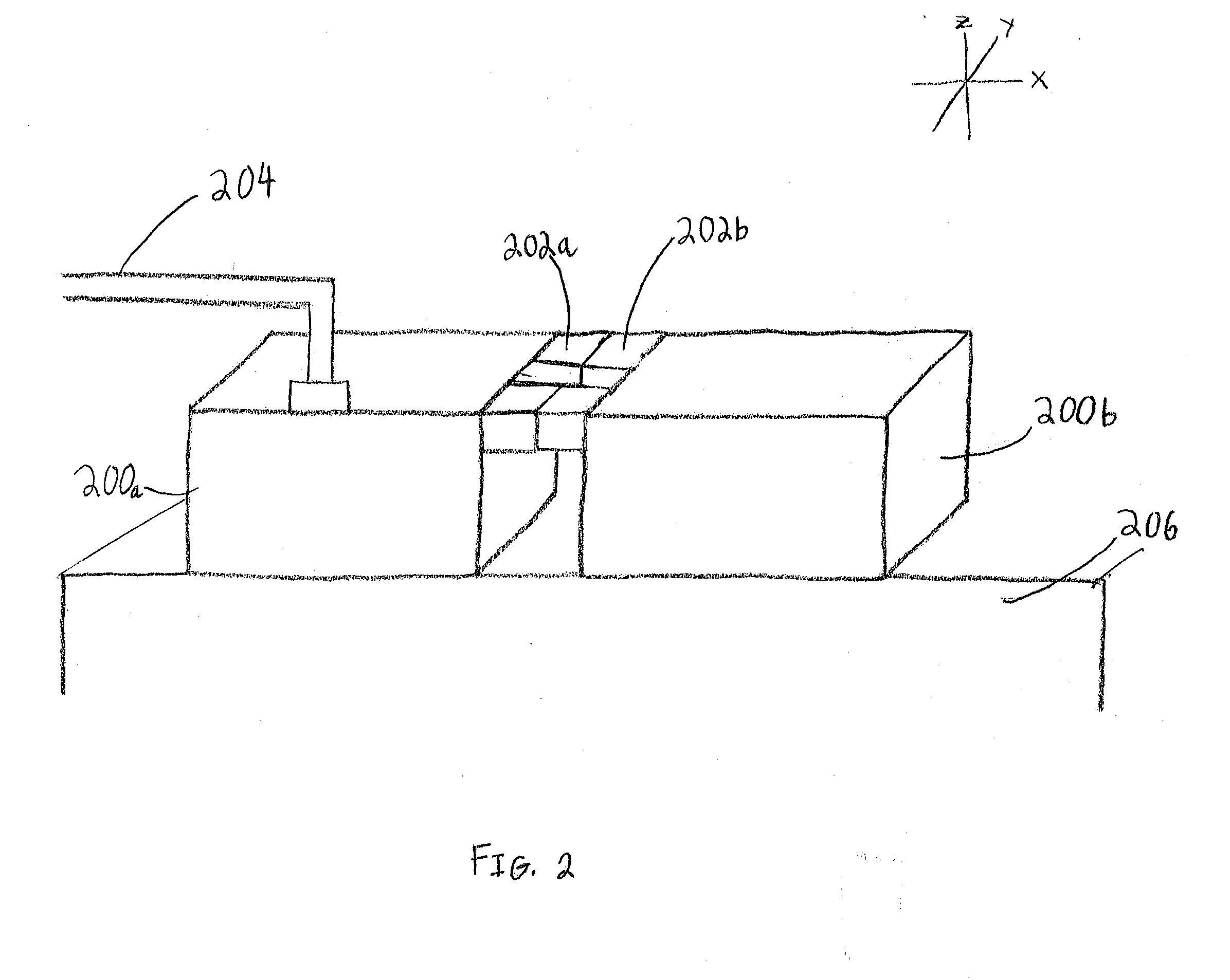
Apparatuses and methods related to the field of microchip assembly and handling, in particular to devices and methods for assembling and handling microchips manufactured with solid edge-to-edge interconnects, such as Quilt Packaging® interconnect technology. Specialized assembly tools are configured to pick up one or more microchips, place the microchips in a specified location aligned to a substrate, package, or another microchip, and facilitate electrical contact through one of a variety of approaches, including solder reflow. This specialized assembly tooling performs heating functions to reflow solder to establish electrical and mechanical interconnections between multiple microchips. Additionally, the interconnected microchips may be arranged in an arbitrarily large array.

Description

CROSS REFERENCE TO RELATED APPLICATION[0001]This application claims priority from U.S. Provisional Application No. 61 / 802,504, filed Mar. 16, 2013, which is incorporated herein by reference.BACKGROUND OF THE INVENTION[0002]1. Field of the Invention[0003]The described apparatuses and methods relate to the field of microchip handling and assembly. More particularly, the described apparatus and methods relate to the handling and assembly of microchips configured with solid edge-to-edge interconnects.[0004]2. Description of Related Art[0005]Generally, electronic systems are comprised of multiple discrete microchips. These microchips work together, along with other peripheral devices, to accomplish particular tasks. For the system to function, the discrete microchips must be electrically connected, both to each other and to any other components contained within the system. A wide variety of methods presently exists to accomplish this connectivity, including wire-bonding, bump-bonding, fl...

Claims


Application Information

Patent Timeline
IPC IPC(8): H05K3/30H05K1/18
CPCH05K1/18H05K3/30H05K1/181H05K3/34H05K2201/1053Y10T29/49128Y02P70/50H05K1/111
Inventor KULICK, JASON M.LU, TIAN
Owner INDIANA INTEGRATED CIRCUITS
Learn More