

Predictive 3-d virtual fabrication system and method
a virtual fabrication and fabrication system technology, applied in the field of predictive 3d virtual fabrication system and method, can solve the problems of negative or null characterization, long experimental run duration, high cost, etc., and achieve the effect of more physical predictiveness
- Summary
- Abstract
- Description
- Claims
- Application Information
AI Technical Summary
Benefits of technology
Problems solved by technology
Method used
Image

Examples
Embodiment Construction
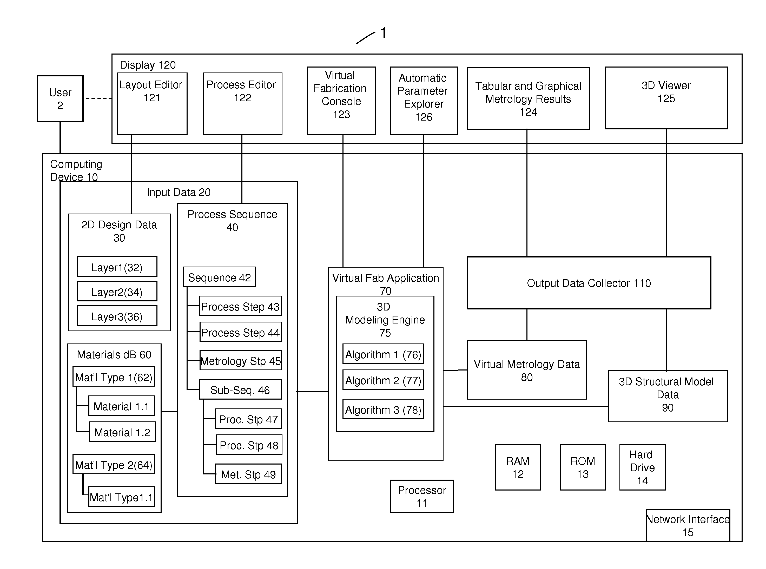
[0036]Embodiments of the present invention provide a faster and more economical approach to semiconductor device structure development. By enhancing a virtual fabrication environment to include the use of virtual metrology measurement data, the effect of alterations in a process or process sequence on device structure can be determined, leading to an optimized fabrication sequence. Further, by calibrating the virtual fabrication environment by comparing virtual metrology data generated from a virtual fabrication run with a subset of measurements performed in a physical fabrication environment, the virtual fabrication environment of the present invention becomes increasingly physically predictive when generating model device structures. Additionally, by conducting virtual experiments in the virtual fabrication environment of the present invention, multiple device structure models may be generated using ranges of process parameters and design parameter variations to cover an entire pr...
PUM
 Abstract
Description
Claims
Application Information