Liquid crystal display and the driving method thereof

a technology of liquid crystal display and driving method, which is applied in the field of display technology, can solve the problems of serious affecting the display performance of tft-lcd, and achieve the effect of enhancing display performance and reducing color shi

Active Publication Date: 2014-10-02
TCL CHINA STAR OPTOELECTRONICS TECH CO LTD
View PDF3 Cites 0 Cited by
  • Summary
  • Abstract
  • Description
  • Claims
  • Application Information

AI Technical Summary

Benefits of technology

[0006]The object of the claimed invention is to provide a liquid crystal display and the driving method to eliminate the voltage difference between the pixel electrodes. In this way, the color shift is reduced, and the display performance of the liquid crystal display is enhanced.
[0024]In view of the above, the waveform shaping circuit shapes the waveforms of the scanning driving signal along the rising edge. The shaped scanning driving signal is transmitted to the pixels via the scanning lines such that the voltage supplied to the pixel electrode of each pixels is similar or the same. In this way, the brightness of the pixels are similar or the same. The color shift is reduced and the display performance is enhanced.

Problems solved by technology

Thus, the display effects of the R pixels and G pixels are not uniformly mixed, which seriously affects display performance of the TFT-LCD.

Method used


Image

  • Liquid crystal display and the driving method thereof
  • Liquid crystal display and the driving method thereof
  • Liquid crystal display and the driving method thereof

Examples


first embodiment

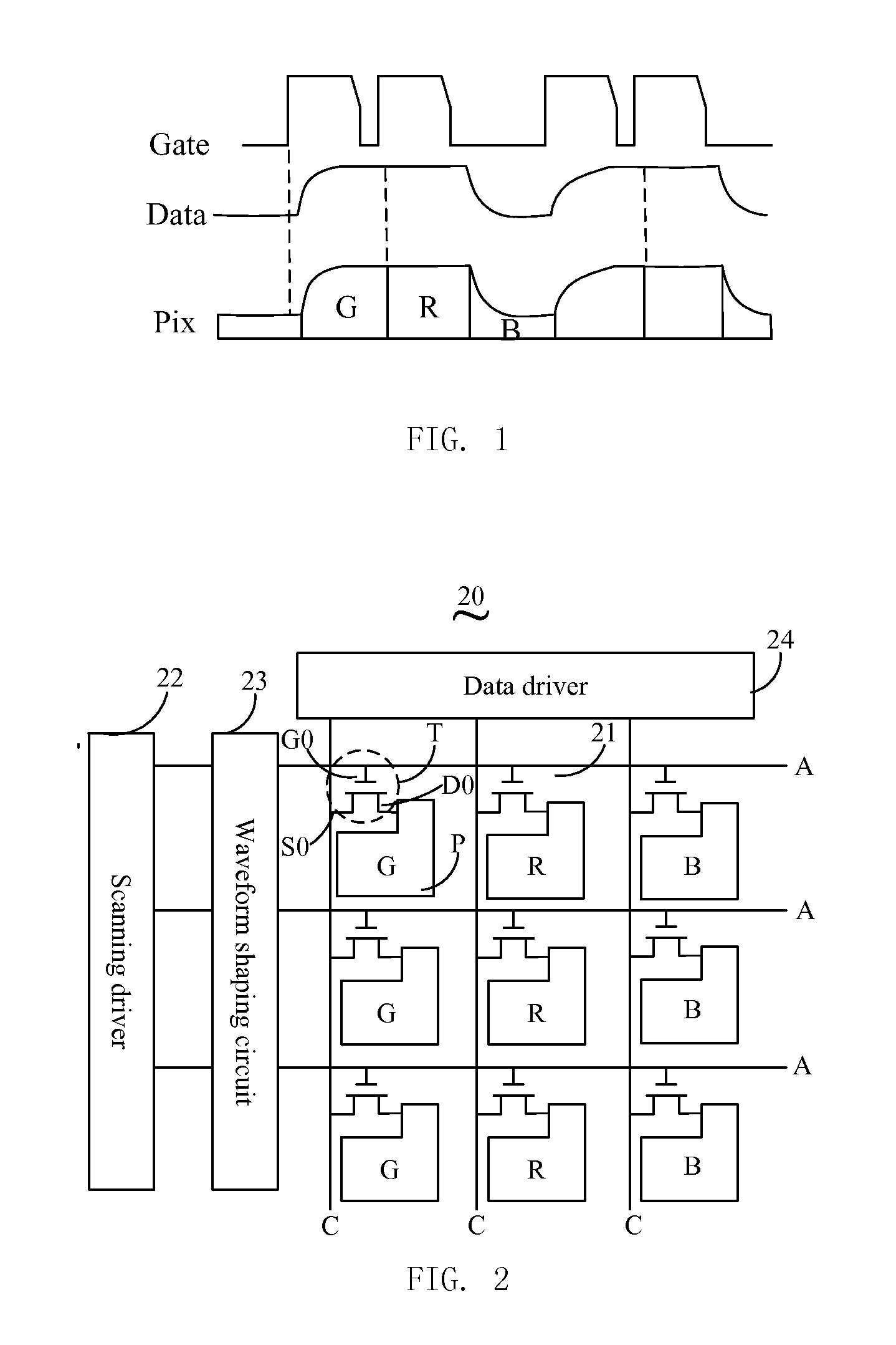
[0032]FIG. 2 is a schematic view of the liquid crystal display in accordance with a The liquid crystal display 20 includes a plurality of pixels 21, a scanning driver 22 for generating scanning driving signals, a waveform shaping circuit 23 connecting with the scanning driver 22, a data driver 24 for generating data driving signals, a plurality of scanning lines (A) and a plurality of data lines (C). The data lines connect to the data driver 24 for transmitting the data driving signals to the pixels 21. The waveform shaping circuit 23 shapes the waveform of the scanning driving signals along the rising edge. The scanning lines connect to the waveform shaping circuit 23 for transmitting the shaped scanning driving signals to the pixels 21.

[0033]In order to reduce the impact toward the horizontal line between two adjacent pixels 21, the waveform shaping circuit 23 further shapes the waveform of the scanning driving signals along the falling edge.

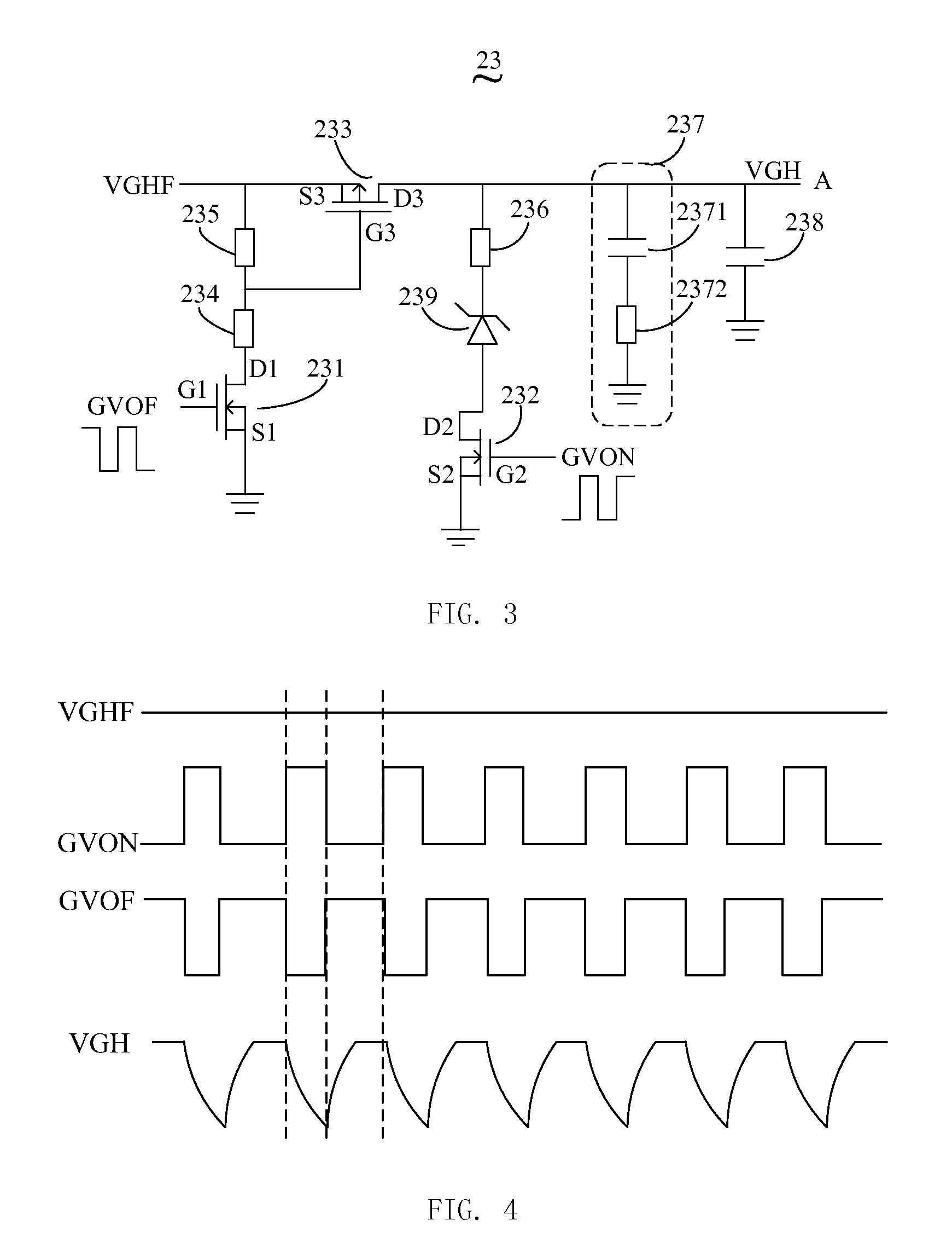
[0034]Specifically, the pixels 21 incl...

second embodiment

[0045]FIG. 6 is a flowchart showing the driving method of the liquid crystal display in accordance with the The driving method includes the following steps. In step S61, the scanning driving signal is provided.

[0046]in step S62 the rising edge of the scanning driving signal is shaped. In order to reduce the impact toward the horizontal line between two adjacent pixels, the waveform of the falling edge of the scanning driving signal is further shaped.

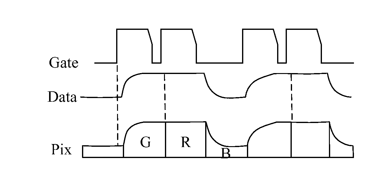
[0047]In step S63, the shaped scanning driving signal is transmitted to the gate of the TFTs by the scanning line so as to turn on the TFTs. When the TFTs are turn on, the scanning driving signal is transmitted to the source of the TFTs by the data lines, and then is further transmitted to the pixel electrodes via the source of the TFTs. The pixel electrodes display according to the received data driving signals. As the waveform of the rising edge of the scanning driving signal is shaped, the time to turn on each of the TFTs (T) is clos...


PUM


Abstract

A liquid crystal display and the driving method thereof are disclosed. The liquid crystal display includes a plurality of pixels, data lines for transmitting data driving signals to the pixels, a scanning driver for generating scanning driving signals, a waveform shaping circuit for connecting with the scanning driver, a plurality of scanning lines for transmitting the shaped scanning driving signal to the pixels. The waveform shaping circuit shapes the waveforms of the scanning driving signal along a rising edge. In this way, the voltage difference between the pixel electrodes is eliminated. Thus, the color shift is reduced, and the display performance of the liquid crystal display is enhanced.

Description

BACKGROUND OF THE INVENTION[0001]1. Field of the Invention[0002]Embodiments of the present disclosure relate to display technology, and more particularly to a liquid crystal display and the driving method thereof.[0003]2. Discussion of the Related Art[0004]FIG. 1 is a waveform diagram showing scanning driving signals and data driving signals of typical pixels of the same column. As shown in FIG 1, for thin film transistor liquid crystal display (TFT-LCD), scanning lines are for transmitting “Gate” scanning driving signals to TFTs to turn on the TFTs. Data lines are for transmitting the “Data” driving signals to the pixels (“Pix”) to supply the power to the pixels when the TFTs are turn on such that the display of the pixels are controlled. The pixels respectively displays red (R), green (G), and blue (B).[0005]For typical liquid crystal displays, the “Gate” scanning driving signals may be delayed during the transition from the low potential to the high potential due to resistors and...

Claims


Application Information

Patent Timeline
Patent Type & Authority Applications(United States)
IPC IPC(8): G09G3/36G09G3/296
CPCG09G3/296G09G3/3674G09G3/3677G09G2320/0223
Inventor HAN, BINGZHU, JIANGLO, SHIH-HSUN
Owner TCL CHINA STAR OPTOELECTRONICS TECH CO LTD
Why Eureka
Try Eureka