Display device and drive method thereof

a display device and drive method technology, applied in the field of display devices, can solve problems such as brightness unevenness in display screens, and achieve the effects of preventing fluctuation in brightness of display screens, and preventing fluctuation in node potential in pixel circuits during standby periods

Active Publication Date: 2014-10-16
SHARP KK
View PDF3 Cites 14 Cited by
  • Summary
  • Abstract
  • Description
  • Claims
  • Application Information

AI Technical Summary

Benefits of technology

[0022]According to the first or twelfth aspect of the present invention, with respect to a pixel circuit provided by connecting a light emitting element and a drive transistor in series on a current path connecting a power supply line and a conductive member to which a common potential is applied, by applying a potential substantially equal to the common potential to the power supply line in a period from completion of threshold detection to start of light emission, fluctuation in the node potential in the pixel circuit in the standby period can be prevented, and fluctuation in brightness of a display screen can be prevented.
[0023]According to the second or third aspect of the present invention, with respect to a pixel circuit including three transistors, one capacitor, and a light emitting element, by applying a potential substantially equal to the common potential to a power supply line connected to the pixel circuit in a period from completion of threshold detection to start of light emission, fluctuation of the node potential in the pixel circuit in the standby period can be prevented, and fluctuation in brightness of a display screen can be prevented.
[0024]According to fourth aspect of the present invention, by suppressing current flowing through a light emitting element in a standby period, the fluctuation of the node potential in the pixel circuit in the standby period can be prevented, and fluctuation in the brightness of a display screen can be prevented.
[0025]According to the fifth or sixth aspect of the present invention, with respect to a pixel circuit including three transistors, two capacitors, and a light emitting element, by applying a potential substantially equal to the common potential to a power supply line connected to the pixel circuit in a period from completion of threshold detection to start of light emission, fluctuation of the node potential in the pixel circuit in the standby period can be prevented, and fluctuation in brightness of a display screen can be prevented.
[0026]According to the seventh aspect of the present invention, with respect to a pixel circuit including four transistors, one capacitor, and a light emitting element, by applying a potential substantially equal to the common potential to a power supply line connected to the pixel circuit in a period from completion of threshold detection to start of light emission, fluctuation of the node potential in the pixel circuit in the standby period can be prevented, and fluctuation in brightness of a display screen can be prevented.
[0027]According to the eighth or ninth aspect of the present invention, by using two kinds of control lines each connected to pixel circuits in a plurality of rows and one kind of power supply line(s) each connected to the pixel circuits in the plurality of rows, a display device in which light emitting elements in pixel circuits in a plurality of row are made to emit light in the same period can be configured. By using one kind of power supply line(s), the layout area of the power supply line can be reduced.

Problems solved by technology

Since the brightness of the organic EL element changes depending on the amount of current flowing through the organic EL element, when variation occurs in the amount of current flowing through the organic EL element, brightness unevenness occurs in a display screen.

Method used


Image

  • Display device and drive method thereof
  • Display device and drive method thereof
  • Display device and drive method thereof

Examples


first embodiment

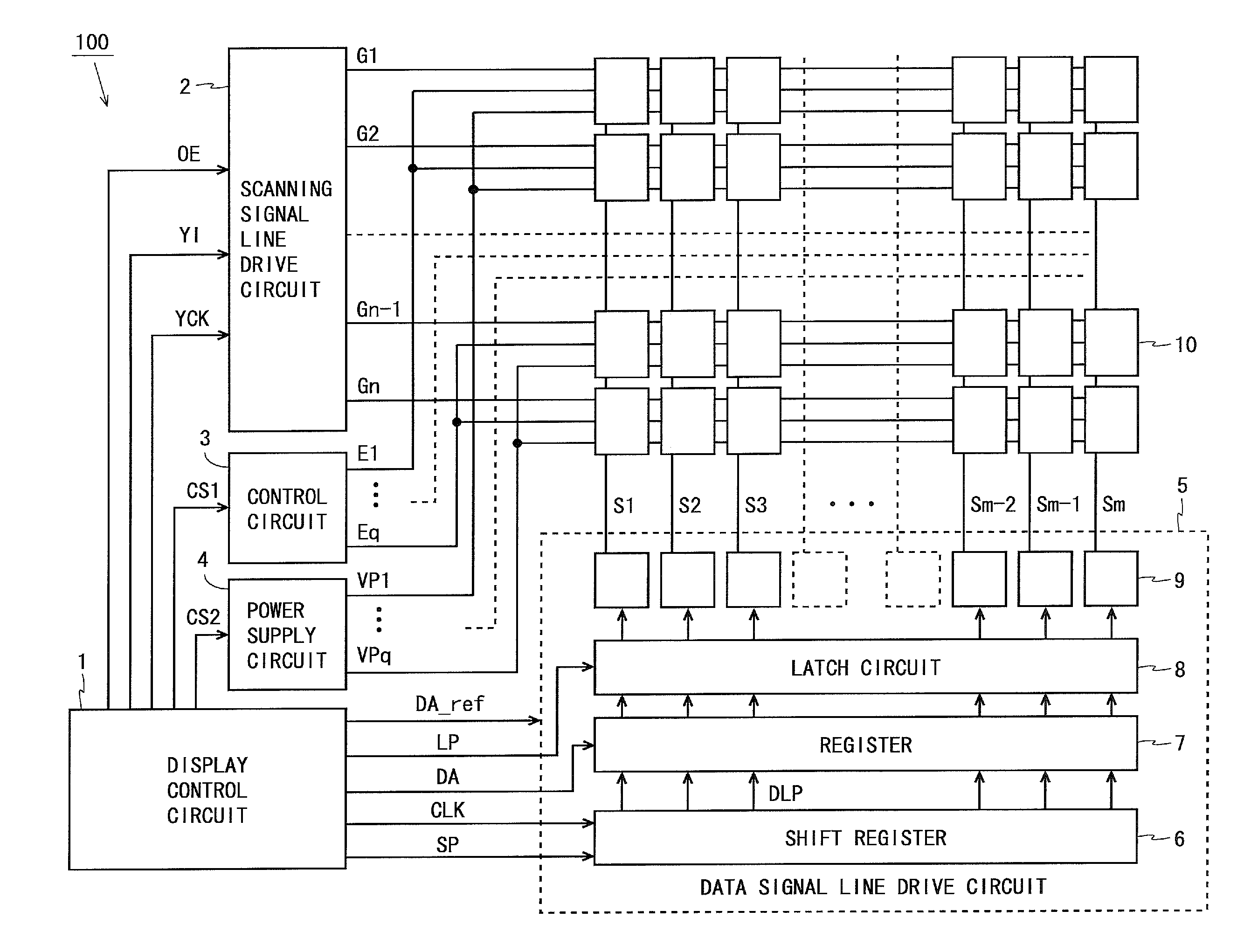
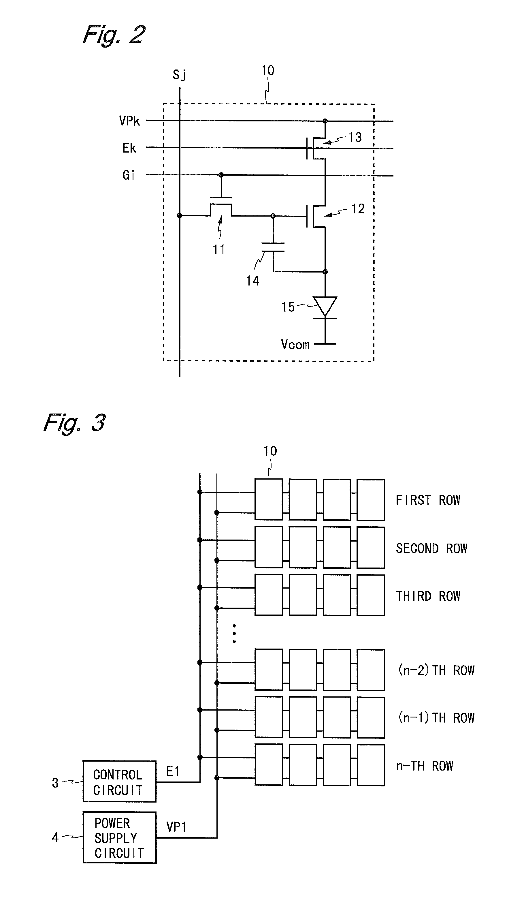
[0053]FIG. 1 is a block diagram illustrating a configuration of a display device according to a first embodiment of the present invention. A display device 100 illustrated in FIG. 1 is an organic EL display having a display control circuit 1, a scanning signal line drive circuit 2, a control circuit 3, a power supply circuit 4, a data signal line drive circuit 5, and (m×n) pieces of pixel circuits 10. The organic EL display is a kind of a current drive type display device. Hereinbelow, each of m and n is an integer of two or larger, each of i and q is an integer which is equal to or larger than one and is equal to or smaller than n, j is an integer which is equal to or larger than one and equal to or smaller than m, and k is an integer which is equal to or larger than one and is equal to or smaller than q.

[0054]The display device 100 is provided with n pieces of scanning signal lines G1 to Gn and m pieces of data signal lines S1 to Sm. The scanning signal lines G1 to Gn are disposed...

second embodiment

[0109]FIG. 12 is a block diagram illustrating a configuration of a display device according to a second embodiment of the present invention. A display device 200 illustrated in FIG. 12 is an organic EL display having the display control circuit 1, the scanning signal line drive circuit 2, a control circuit 203, a power supply circuit 204, the data signal line drive circuit 5, and (m×n) pieces of pixel circuits 20. In the following embodiments, the same reference numerals are designated to the same components as those of the foregoing embodiment and their description will be omitted. Hereinafter, the points different from the display device 100 of the first embodiment will be described.

[0110]The display device 200 is provided with q pieces of control lines AZ1 to AZq, as control lines. The pixel circuits 20 in each row are connected to one of the control lines AZ1 to AZq and one of the power supply lines VP1 to VPq. To the pixel circuit 20, the common potential Vcom is supplied by us...

third embodiment

[0142]FIG. 15 is a block diagram illustrating a configuration of a display device according to a third embodiment of the present invention. A display device 300 illustrated in FIG. 15 is an organic EL display having the display control circuit 1, the scanning signal line drive circuit 2, a control circuit 303, a power supply circuit 304, the data signal line drive circuit 5, and (m×n) pieces of pixel circuits 30. Hereinafter, the points different from the display device 100 of the first embodiment will be described.

[0143]The display device 300 is provided with, as control lines, q pieces of control lines E1 to Eq and q pieces of control lines AZ1 to AZq. The pixel circuits 30 in each row are connected to one of the control lines E1 to Eq, one of the control lines AZ1 to AZq and one of the power supply lines VP1 to VPq. To the pixel circuit 30, the common potential Vcom is supplied by using a not-illustrated conductive member (electrode).

[0144]The control circuit 303 selectively appl...


PUM


Abstract

A pixel circuit 10 is provided with TFTs 12 and 13 and an organic EL element 15 on a current path connecting a power supply line VPk and an electrode having a common potential Vcom. A display device 100 simultaneously performs initialization to pixel circuits 10 in a plurality of rows, simultaneously perform threshold detection to the pixel circuits 10 in the plurality of rows, sequentially writes data to the pixel circuits 10 row by row, and makes the organic EL elements 15 included in the pixel circuits 10 in the plurality of rows emit light in the same period. In a period from completion of threshold detection to start of light emission, the TFTs 11 and 13 are controlled to an off state, and a potential VP_C which is substantially equal to the common potential Vcom is applied to the power supply line VPk. Consequently, leak current flowing through the TFTs 12 and 13 can be suppressed, and the fluctuation in the node potential in the pixel circuit 10 in a standby period can be prevented.

Description

TECHNICAL FIELD[0001]The present invention relates to a display device and, more specifically, to a current drive type display device such as an organic EL display and a drive method of the same.BACKGROUND ART[0002]As a thin, high picture quality, and low power consumption display device, an organic EL (Electro Luminescence) display has been known. The organic EL display has a plurality of pixel circuits each including an organic EL element, a drive transistor, and a control transistor. As transistors in each pixel circuit, thin film transistors (hereinbelow, referred to as TFTs) are used.[0003]In an organic EL display, variation occurs in a threshold voltage and a mobility of a drive transistor in a pixel circuit. Due to this, even when the same data potential is written to the pixel circuits, variation occurs in the amount of current flowing through the organic EL elements. Since the brightness of the organic EL element changes depending on the amount of current flowing through th...

Claims


Application Information

Patent Timeline
Patent Type & Authority Applications(United States)
IPC IPC(8): G09G3/32
CPCG09G3/3233G09G3/3241G09G2300/0861G09G2300/0852
Inventor KISHI, NORITAKA
Owner SHARP KK
Why Eureka
Try Eureka