Display device, driving method of the same and electronic equipment having the same

a technology of electronic equipment and drive transistor, which is applied in the direction of static indicating devices, instruments, electroluminescent light sources, etc., can solve the problems of reducing the pixel size, and achieve the effect of suppressing the reduction of the gate the reduction of the gate-to-source voltage of the drive transistor

Inactive Publication Date: 2008-07-31
JOLED INC
View PDF2 Cites 11 Cited by
  • Summary
  • Abstract
  • Description
  • Claims
  • Application Information

AI Technical Summary

Benefits of technology

[0014]This technique makes it possible to configure a pixel circuit with the minimum required number of elements. That is, a pixel circuit can be made up of a write transistor adapted to sample an input signal voltage and write the voltage to the pixel, a holding capacitance adapted to hold the input signal voltage written by the write transistor, and a drive transistor adapted to drive the electro-optical element based on the input signal voltage held by the holding capacitance.
[0019]It is also desirable to provide a display device capable of writing the input signal voltage in a stable manner while at the same time preventing the brightness being declined with the reduction of the gate-to-source voltage of the drive transistor due to coupling when the write transistor turns off, a driving method of the same and electronic equipment having the same.
[0023]In the display device configured as described above and electronic equipment having the same, the supply voltage supplied to the power supply of the final stage buffer has a slower fall time than that of the input pulse to the final stage buffer. As a result, the write pulse from the final stage buffer is slower than that of the input pulse. That is, the write pulse falls slowly. This suppresses the reduction of the gate voltage of the drive transistor due to coupling when the write transistor turns off. As a result, the reduction of the gate-to-source voltage of the drive transistor can be suppressed.

Problems solved by technology

However, each pixel circuit includes a large number of elements, thus posing a hurdle for the reduction of the pixel size.

Method used


Image

  • Display device, driving method of the same and electronic equipment having the same
  • Display device, driving method of the same and electronic equipment having the same
  • Display device, driving method of the same and electronic equipment having the same

Examples


embodiment 1

[0112]A description will be given below about a concrete embodiment adapted to produce a steeply rising leading edge of the scan signal WS.

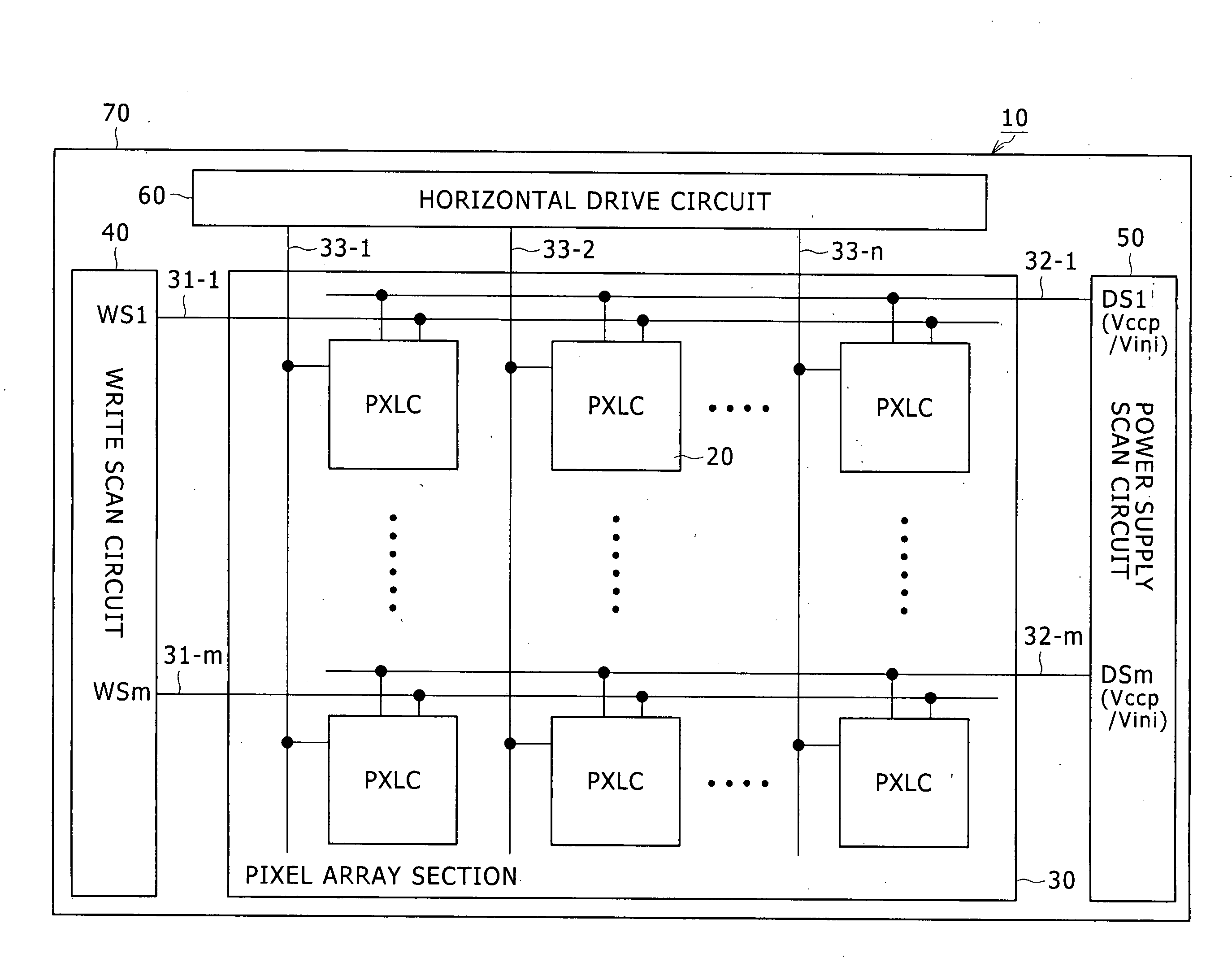
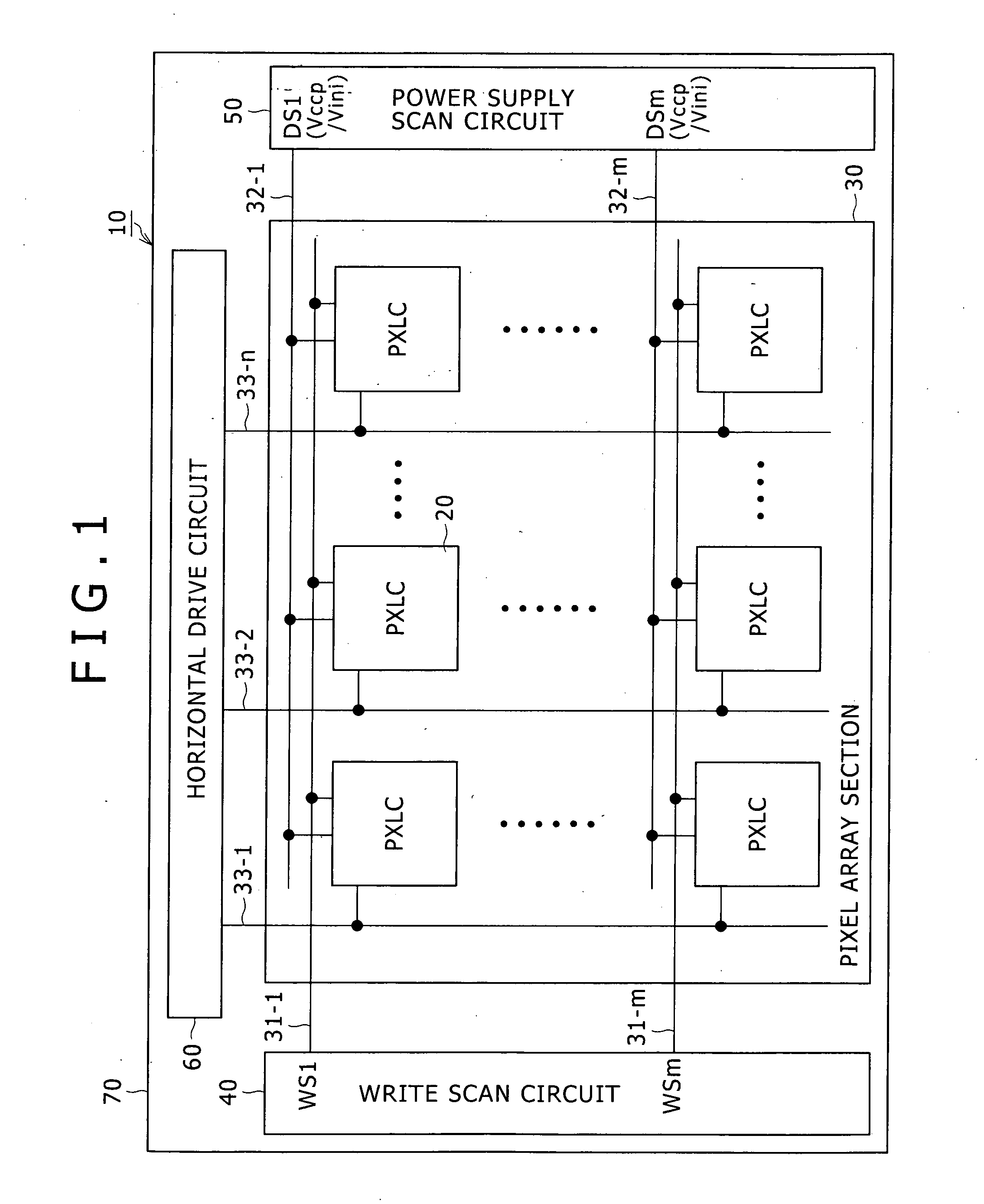
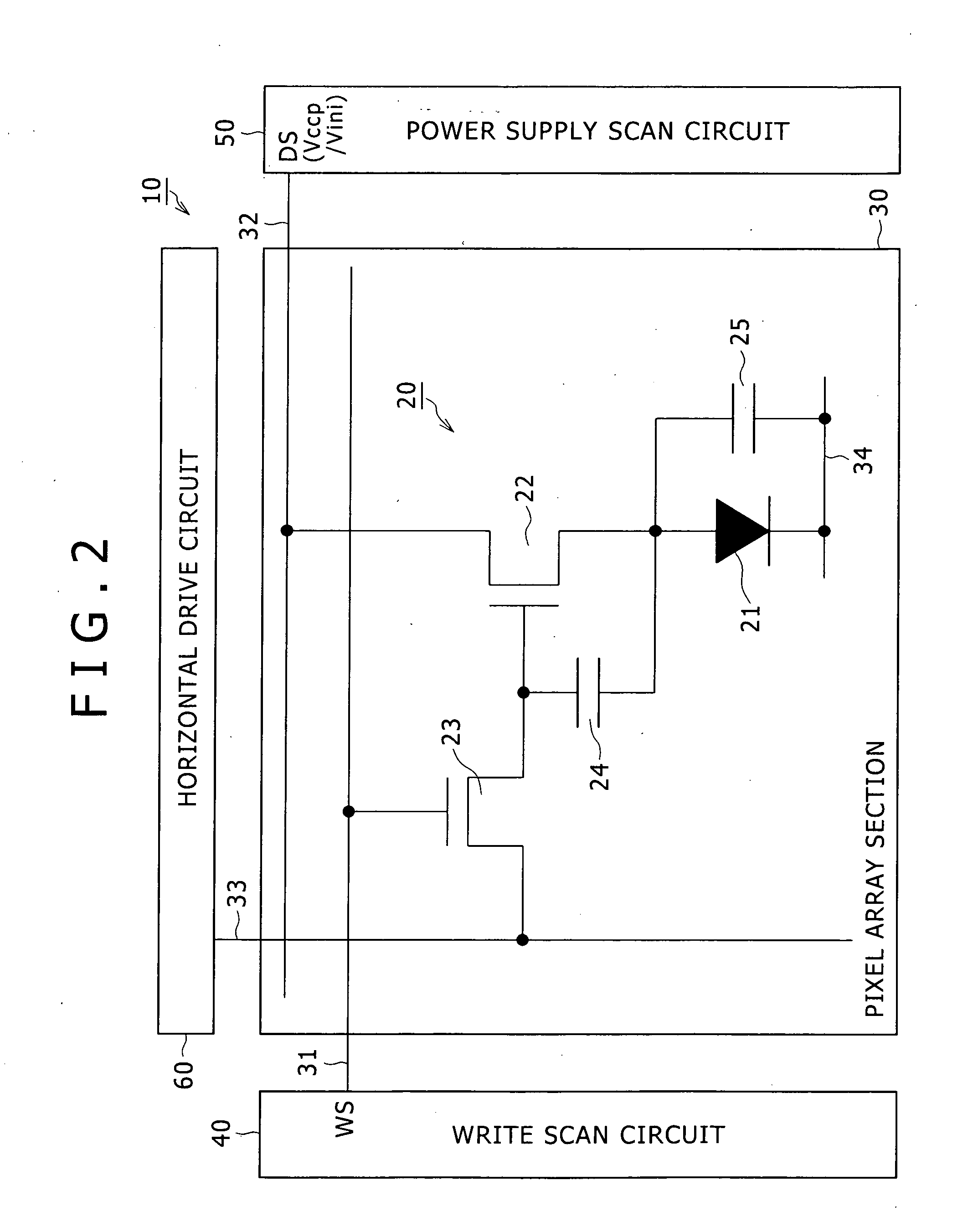
[0113]As mentioned earlier, the scan signal WS (any of WS1 to WSm) is output from the write scan circuit 40. The write scan circuit 40 includes a shift register 41, a logic circuit 42 and an output circuit 43 as illustrated in FIG. 12. The output circuit 43 includes a plurality of stages of buffers for each pixel row. The write scan circuit 40 is incorporated on the display panel 70 as a drive section adapted to drive the pixels 20 of the pixel array section 30.

[0114]The write scan circuit 40 is supplied with a timing signal and supply voltage from a control board 80 provided externally to the display panel 70, for example, via a flexible cable 90. More specifically, the control board 80 has components such as a timing generator 81, a Vdd1 power supply circuit 82 and a Vdd2 power supply circuit 83.

[0115]The timing generator 81 generates a clock p...

embodiment 2

[0131]A description will be given next about a concrete embodiment adapted to produce a slowly falling trailing edge of the write pulse which is adapted to write the input signal voltage Vsig (scan signal WS in the latter half).

[0132]As mentioned earlier, the scan signal WS (any of WS1 to WSm) is output from the write scan circuit 40. The write scan circuit 40 includes the shift register 41, the logic circuit 42 and the output circuit 43 as illustrated in FIG. 16. The output circuit 43 includes a plurality of stages of buffers for each pixel row. The write scan circuit 40 is incorporated on the display panel 70 as a drive section adapted to drive the pixels 20 of the pixel array section 30.

[0133]The write scan circuit 40 is supplied with a timing signal and supply voltage from the control board 80 provided externally to the display panel 70, for example, via the flexible cable 90. More specifically, the control board 80 has components such as the timing generator 81, the Vdd1 power ...

application examples

[0178]The aforementioned display device according to an embodiment of the present invention is applicable to display devices of electronic equipment used in all fields which is designed to display the image or video of the video signal generated therein. Among such electronic equipment are a wide variety of different equipment illustrated in FIGS. 23 to 27, namely, a digital camera, laptop personal computer, mobile terminal device such as mobile phone, and video camcorder. A description will be given below about examples of electronic equipment to which an embodiment according to the present invention is applied.

[0179]It should be noted that among the display devices according to an embodiment of the present invention are those in a modular form having a sealed configuration. A display device which fits into this category is a display module formed by attaching a transparent opposed section made of glass or other material to the pixel array section 30. This transparent opposed secti...


PUM


Abstract

A pixel circuit of a display device of the present invention has a drive transistor which serves also as a transistor adapted to control the emission and non-emission periods of an organic EL element or other elements. A final stage buffer in an output circuit of a write scan circuit (WS) has its power supply separated from the power supply of circuit portions of a previous stage. In a first embodiment, a scan signal WS from the write scan circuit is activated instantaneously. In a second embodiment, the trailing edge of the scan signal WS falls slowly. This allows for writing of an input signal voltage in a stable manner.

Description

CROSS REFERENCES TO RELATED APPLICATIONS[0001]The present invention contains subject matter related to Japanese Patent Application JP 2007-015965 filed in the Japan Patent Office on Jan. 26, 2007, and to Japanese Patent Application JP 2007-023892 filed in the Japan Patent Office on Feb. 2, 2007, the entire contents of which being incorporated herein by reference.BACKGROUND OF THE INVENTION[0002]1. Field of the Invention[0003]The present invention relates to a display device, a driving method of the same and electronic equipment. The present invention relates particularly to a flat panel display device having pixels including electro-optical elements arranged in a matrix form, a driving method of the same and electronic equipment having the same.[0004]2. Description of the Related Art[0005]In the field of image display devices, recent years have seen the development and commercialization of flat panel display devices having pixels including light-emitting elements arranged in a matri...

Claims


Application Information

Patent Timeline
Patent Type & Authority Applications(United States)
IPC IPC(8): G09G3/20
CPCG09G3/3233G09G3/3266G09G2300/0819G09G2300/0852H01L27/3244G09G2320/0233G09G2330/028G11C19/28G09G2310/066H10K59/12G09G3/30G09G3/32G09G3/20H05B33/12
Inventor MINAMI, TETSUOUCHINO, KATSUHIDEIIDA, YUKIHITO
Owner JOLED INC
Why Eureka
Try Eureka