

Light Emitting Key
a technology of light emitting keys and pressure-sensitive sensors, which is applied in the direction of resistors, adjustable resistors, contacts, etc., can solve the problem that pressure-sensitive sensors b>1/b> cannot be seen clearly in a dark environmen
- Summary
- Abstract
- Description
- Claims
- Application Information
AI Technical Summary
Benefits of technology
Problems solved by technology
Method used
Image

Examples
first embodiment
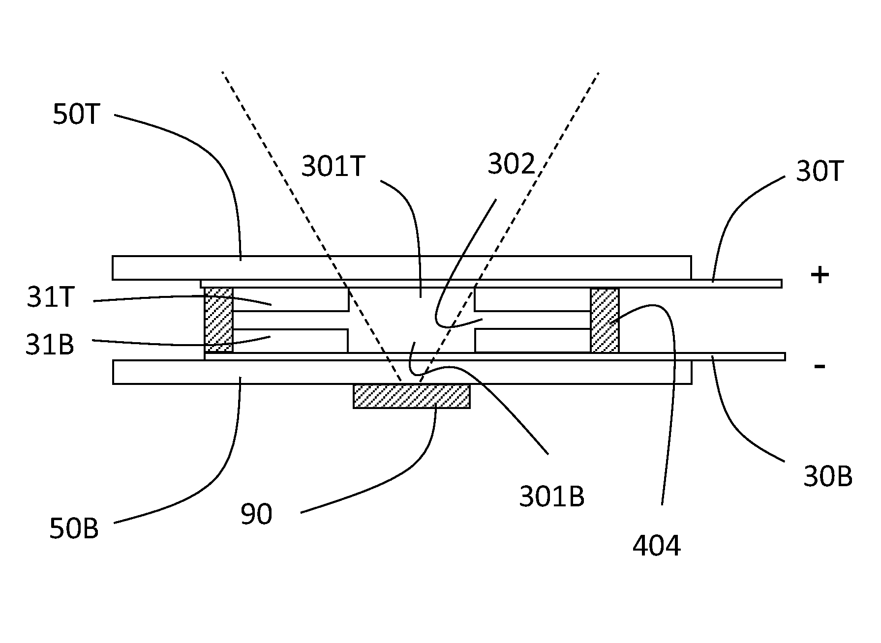
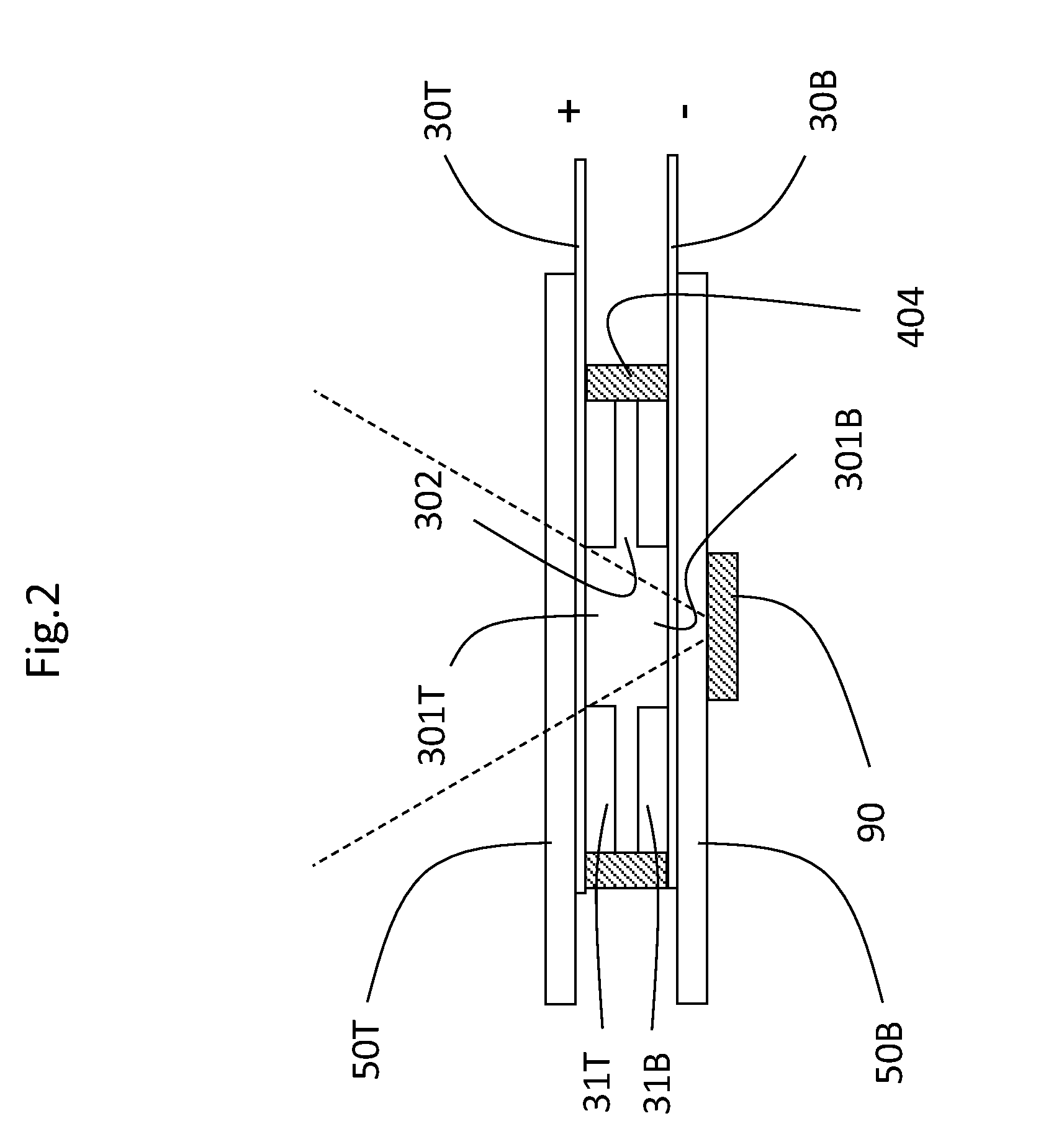
[0021]FIG. 2 shows a light emitting key according to the present invention.
[0022]FIG. 2 shows a section view of a first embodiment for a light emitting key. A top transparent substrate 50T is prepared. A top electrode 30T is configured under the top substrate 50T. A top piezo piezoresistive layer 31T is configured on a bottom of the top electrode 30T. A bottom piezoresistive layer 31B is configured under the top piezoresistive layer 31T but maintains a space 302 therebetween. A bottom electrode 30B is configured on a bottom of the bottom piezoresistive layer 31B. A top through hole 301T is made through the top piezoresistive layer 31T. A bottom through hole 301B is made through the bottom piezoresistive layer 31B. A pair of spacers 404 is configured between the top electrode 30T and the bottom electrode 30B so that the gap 302 is formed between the top piezoresistive layer 31T and the bottom piezoresistive layer 31B. A bottom substrate 50B is configured on the bottom of the bottom e...
second embodiment
[0027]FIG. 4 shows a light emitting key according to the present invention
[0028]FIG. 4 shows a light emitting key having a cruciform ditch 401 made through the top electrode 40T, the top piezoresistive layer 41T, the bottom piezoresistive layer 41B, and the bottom electrode 40B. In this embodiment, four top stacks and four bottom stacks occupy the outer four corners of the cruciform ditch 401. The four top electrodes 40T of the four top stacks are electrically coupled to a first electrode 701, say, a positive electrode. The four bottom electrodes 40B of the four bottom stacks are electrically coupled to a second electrode 702, say, a negative electrode. A light source 90 is then configured under the bottom to make the whole structure a single light emitting key.
[0029]FIG. 5A shows a top view of FIG. 4
[0030]FIG. 5A shows that a cruciform ditch 401 is made for light emitting. Four stacks occupy the outer four corners of the cruciform ditch 401. Each block includes a top electrode 40T,...
third embodiment
[0043]FIG. 9 shows a light emitting key according to the present invention
[0044]FIG. 9 shows single piezoresistive layer 31 is used. The basic principle is the same as described above. A top substrate 50T is prepared. A top electrode 30T is made on a bottom of the top substrate 50T. A piezoresistor layer 31 is made on a bottom of the top electrode 30T. A gap 402 is reserved under the piezoresistive layer 31. A bottom electrode 30B is made under the gap 302. A bottom substrate 50B is made on a bottom of the bottom electrode 30B. A spacer 404 is configured between the top substrate 50T and the bottom substrate 50B. A light source 90, such as a light emitted diode (LED), is arranged under the bottom substrate 50B. A rectangular through hole is made through the piezoresistive layer 31. When the light emitted diode 90 is turned on, light beams shall emit from area 601 on the top substrate 50T.
[0045]The space 302 is made between the piezoresistive layer 31 and the bottom electrode 30B, th...
PUM
 Abstract
Description
Claims
Application Information