Organic light emitting diode display

a light-emitting diode and organic technology, applied in the field of organic light-emitting diodes (oled) displays, can solve the problems of reducing the size of each pixel, affecting the resolution of the display, and exposing the object to particles at a shorter distance, so as to achieve high resolution

Active Publication Date: 2014-12-04
SAMSUNG DISPLAY CO LTD
View PDF2 Cites 54 Cited by
  • Summary
  • Abstract
  • Description
  • Claims
  • Application Information

AI Technical Summary

Benefits of technology

[0010]Exemplary embodiments of the present invention relates to an organic light emitting diode (OLED...

Problems solved by technology

Also, as the organic light emitting diode (OLED) display becomes high resolution, the size of each pixel is decreased such that an interval between the driving voltage line and the data line ...

Method used


Image

  • Organic light emitting diode display
  • Organic light emitting diode display
  • Organic light emitting diode display

Examples


Embodiment Construction

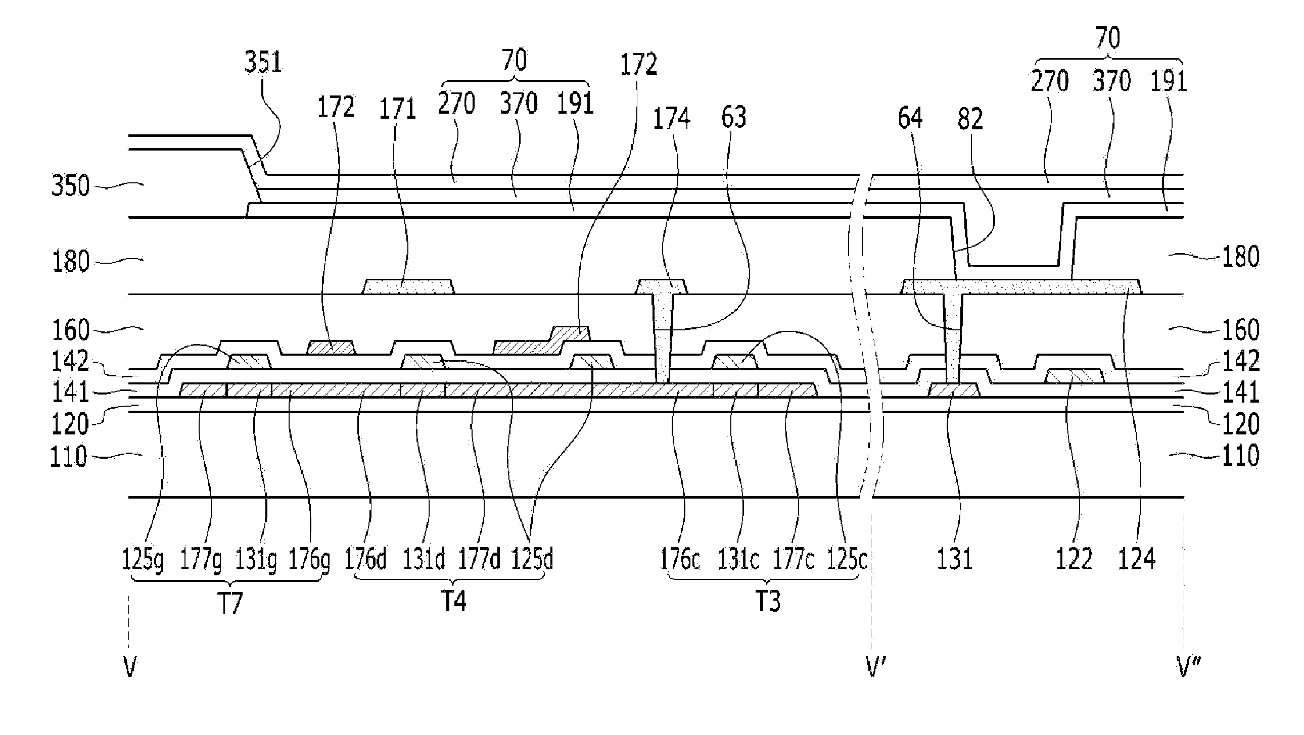
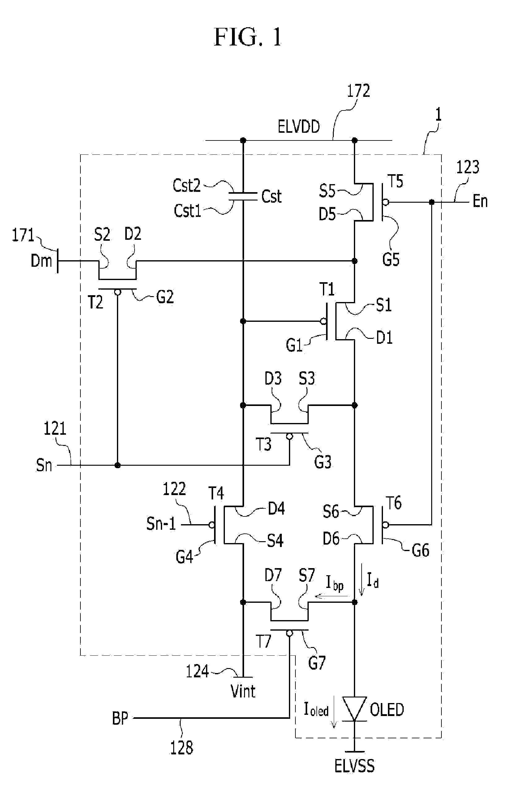
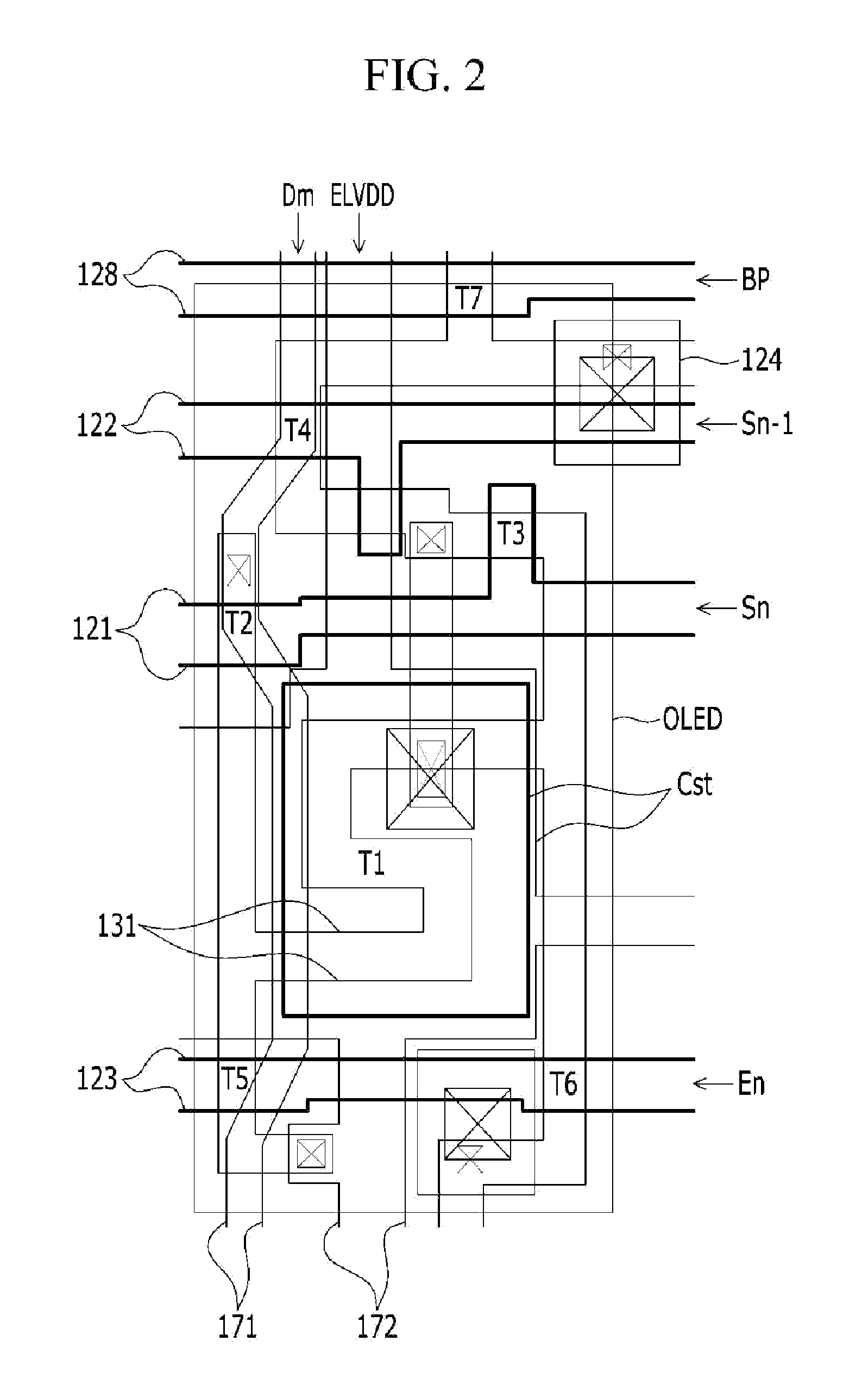
[0023]The invention is described more fully hereinafter with reference to the accompanying drawings, in which exemplary embodiments of the invention are shown. This invention may, however, be embodied in many different forms and should not be construed as limited to the exemplary embodiments set forth herein. Rather, these exemplary embodiments are provided so that this disclosure is thorough, and will fully convey the scope of the invention to those skilled in the art. In the drawings, the size and relative sizes of layers and regions may be exaggerated for clarity. Like reference numerals in the drawings denote like elements.

[0024]In addition, the size and thickness of each configuration shown in the drawings are arbitrarily shown for better understanding and ease of description, but the present invention is not limited thereto.

[0025]In the drawings, the thickness of layers, films, panels, regions, etc., are exaggerated for clarity. In the drawings, for understanding and ease of d...


PUM


Abstract

An organic light emitting diode (OLED) display including: a substrate; a semiconductor layer disposed on the substrate and including a switching semiconductor layer and a driving semiconductor layer connected to the switching semiconductor layer; a first gate insulating layer disposed on the semiconductor layer; a switching gate electrode and a driving gate electrode disposed on the first gate insulating layer and respectively overlapping with the switching semiconductor layer and the driving semiconductor layer; a second gate insulating layer disposed on the switching gate electrode and the driving gate electrode; a driving voltage line configured to transmit a driving voltage and disposed on the second gate insulating layer; an interlayer insulating layer disposed on the driving voltage line and the second gate insulating layer; and a data line configured to transmit a data signal and disposed on the interlayer insulating layer.

Description

CROSS-REFERENCE TO RELATED APPLICATION[0001]This application claims priority to and the benefit of Korean Patent Application No. 10-2013-0062058 filed in the Korean Intellectual Property Office on May 30, 2013, the entire contents of which are incorporated herein by reference.BACKGROUND OF THE INVENTION[0002]1. Field[0003]Exemplary embodiments of the present invention relate to an organic light emitting diode (OLED) display.[0004]2. Discussion of the Background[0005]An organic light emitting diode display includes two electrodes and an organic emission layer interposed therebetween, wherein electrons injected from a cathode that is one electrode and holes injected from an anode that is the other electrode are bonded to each other in the organic emission layer to form excitons, and light is emitted while the excitons discharge energy.[0006]The organic light emitting diode display includes a plurality of pixels including an organic light emitting diode that is formed of a cathode, an ...

Claims


Application Information

Patent Timeline
IPC IPC(8): H01L27/32
CPCH01L27/3265H01L27/3262H10K59/1216H10K59/1213H10K59/131G09F9/301G09G3/3208H10K59/10H10K59/125H10K50/805
Inventor JIN, MIN-HYUN
Owner SAMSUNG DISPLAY CO LTD
Why Eureka
Try Eureka