Wafer carrier having thermal uniformity-enhancing features

a technology of thermal uniformity and carrier, which is applied in the field of wafer processing apparatus, can solve the problems of unfavorable variations in the properties of the resulting semiconductor device, and achieve the effect of limiting heat flow and avoiding historic flow heating effects

Inactive Publication Date: 2014-12-11
VEECO INSTR
View PDF6 Cites 178 Cited by
  • Summary
  • Abstract
  • Description
  • Claims
  • Application Information

AI Technical Summary

Benefits of technology

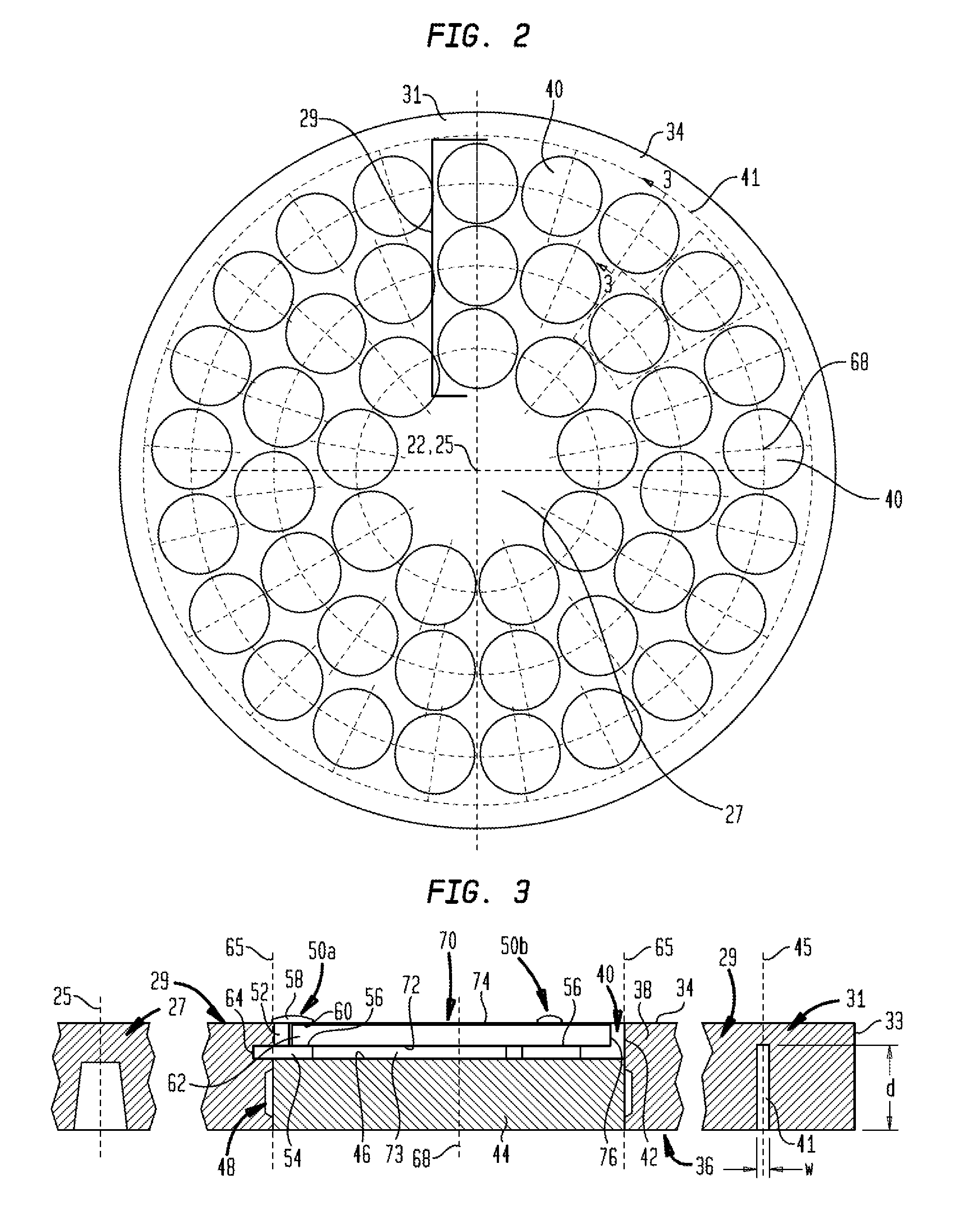
[0010]In another embodiment, the thermal control features are specifically situated beneath the regions of the wafer carrier that are between the wafer pockets. These thermal control features limit the heat flow to the surface of these regions, thereby keeping those surface portions relatively cooler. In one type of embodiment, the surface temperature of the regions between the pockets is maintained at approximately the temperature of the wafers, thereby avoiding historic flow heating effects.

Problems solved by technology

Minor variations in composition of the reactive gases and in the temperature of the wafer surfaces cause undesired variations in the properties of the resulting semiconductor device.

Method used


Image

  • Wafer carrier having thermal uniformity-enhancing features
  • Wafer carrier having thermal uniformity-enhancing features
  • Wafer carrier having thermal uniformity-enhancing features

Examples


Embodiment Construction

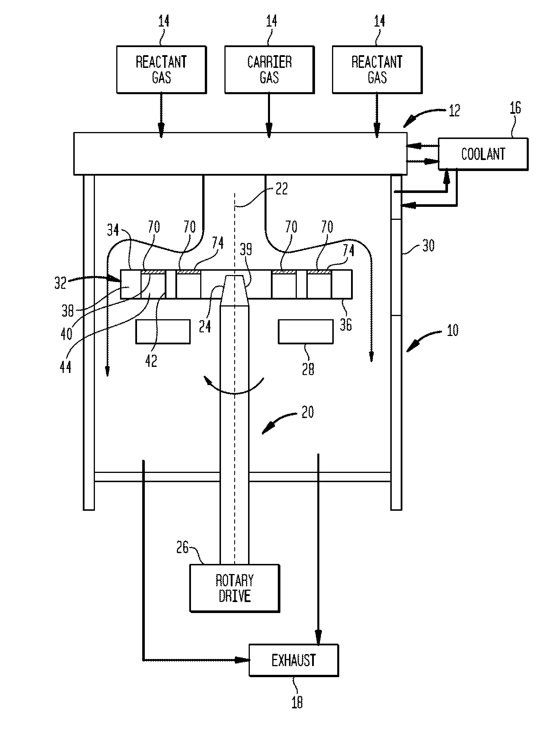
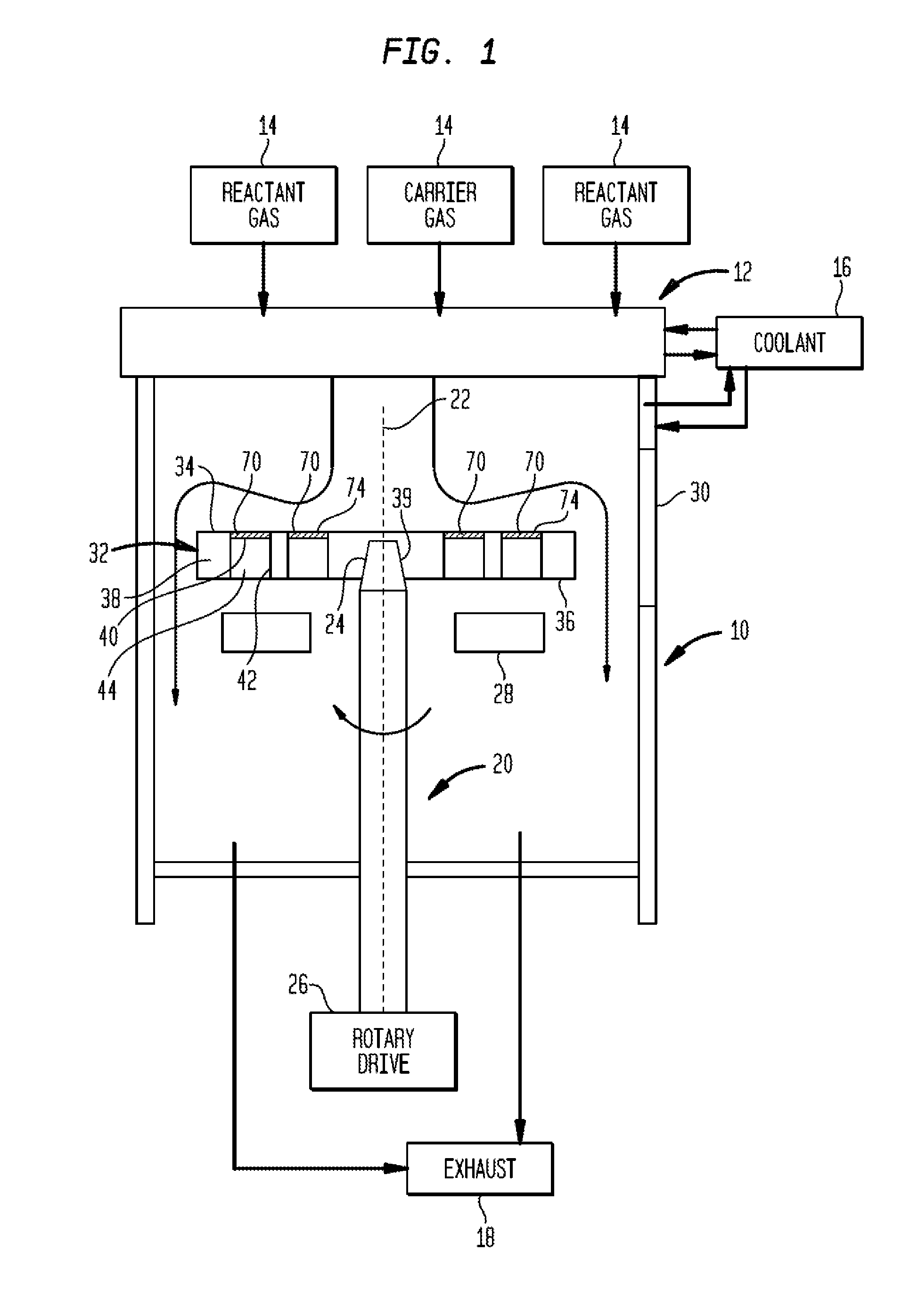
[0042]Chemical vapor deposition apparatus in accordance with one embodiment of the invention includes a reaction chamber 10 having a gas distribution element 12 arranged at one end of the chamber. The end having the gas distribution element 12 is referred to herein as the “top” end of the chamber 10. This end of the chamber typically, but not necessarily, is disposed at the top of the chamber in the normal gravitational frame of reference. Thus, the downward direction as used herein refers to the direction away from the gas distribution element 12 and the upward direction refers to the direction within the chamber, toward the gas distribution element 12, regardless of whether these directions are aligned with the gravitational upward and downward directions. Similarly, the “top” and “bottom” surfaces of elements are described herein with reference to the frame of reference of chamber 10 and element 12.

[0043]Gas distribution element 12 is connected to sources 14 of gases to be used i...


PUM

PropertyMeasurementUnit
temperatureaaaaaaaaaa
thicknessaaaaaaaaaa
diameteraaaaaaaaaa

Abstract

A wafer carrier assembly for use in a system for growing epitaxial layers on one or more wafers by chemical vapor deposition (CVD), the wafer carrier assembly includes a wafer carrier body formed symmetrically about a central axis, and including a generally planar top surface that is situated perpendicularly to the central axis and a planar bottom surface that is parallel to the top surface. At least one wafer retention pocket is recessed in the wafer carrier body from the top surface. Each of the at least one wafer retention pocket includes a floor surface and a peripheral wall surface that surrounds the floor surface and defines a periphery of that wafer retention pocket. At least one thermal control feature includes an interior cavity or void formed in the wafer carrier body and is defined by interior surfaces of the wafer carrier body.

Description

PRIOR APPLICATION[0001]This application claims the benefit of U.S. Provisional Application No. 61 / 831,496, filed Jun. 5, 2013, the disclosure of which is incorporated by reference herein.BACKGROUND OF THE INVENTION[0002]The present invention relates to wafer processing apparatus, to wafer carriers for use in such processing apparatus, and to methods of wafer processing.[0003]Many semiconductor devices are formed by epitaxial growth of a semiconductor material on a substrate. The substrate typically is a crystalline material in the form of a disc, commonly referred to as a “wafer.” For example, devices formed from compound semiconductors such as III-V semiconductors typically are formed by growing successive layers of the compound semiconductor using metal organic chemical vapor deposition or “MOCVD.” In this process, the wafers are exposed to a combination of gases, typically including a metal organic compound and a source of a group V element which flow over the surface of the wafe...

Claims


Application Information

Patent Timeline
Patent Type & Authority Applications(United States)
IPC IPC(8): C30B25/10C30B25/12
CPCC30B25/12C30B25/105C23C16/4586Y10T29/49826C23C16/4584C23C16/46
Inventor ARMOUR, ERICKRISHNAN, SANDEEPZHANG, ALEXMITROVIC, BOJANGURARY, ALEXANDER
Owner VEECO INSTR
Why Eureka
Try Eureka