
Magnetic sensor and method of manufacture thereof

a technology of magnetic sensor and manufacturing method, which is applied in the field of magnetic sensor, can solve the problems of deteriorating the sensitivity of the magnetic sensor, high possibility of malfunction,

Active Publication Date: 2014-12-18
MAGNACHIP SEMICONDUCTOR LTD
View PDF2 Cites 23 Cited by
  • Summary
  • Abstract
  • Description
  • Claims
  • Application Information

AI Technical Summary

Benefits of technology

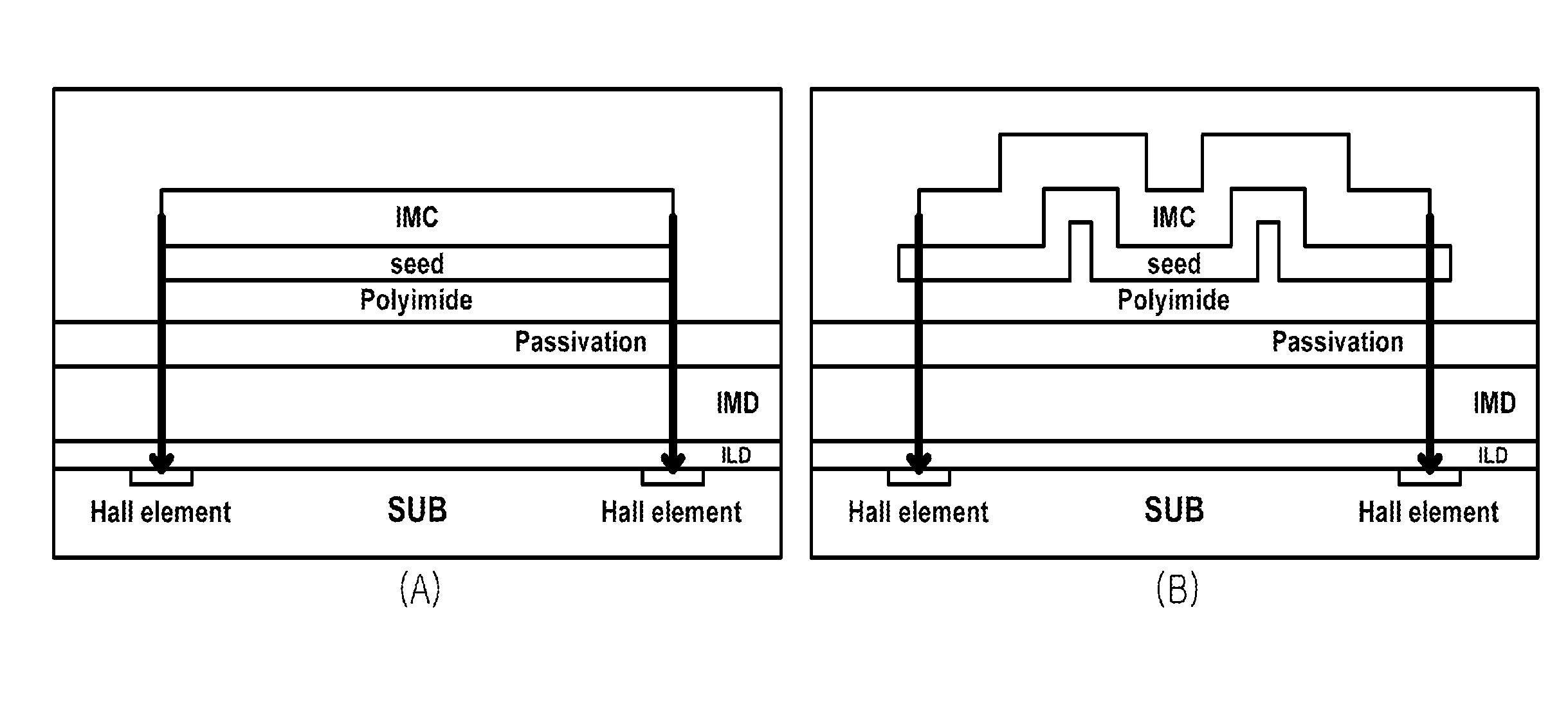
This patent describes a magnetic sensor with a unique design that allows for improved detection and positioning of magnetic fields. The sensor includes a substrate with a plurality of Hall elements, a protective layer, a base layer, and an integrated magnetic concentrator (IMC). The IMC has an elevated surface with a shape that matches the second buffer layer. The sensor also includes a first buffer layer and a second buffer layer, and a protruding portion on the base layer that extends from the outer edge of the IMC. The sensor is advantageous for use in digital compass applications and can be manufactured using various techniques such as photoresist and wet etching. The technical effect of this design is improved magnetic field detection and positioning with improved accuracy and precision.

Problems solved by technology

Higher offset voltage leads into higher possibility of malfunction.
High offset voltage causes minute changes in the actual voltage of the Hall elements in the presence of a magnetic field, and thus deteriorates the sensitivity of the magnetic sensor.

Method used


Image

  • Magnetic sensor and method of manufacture thereof
  • Magnetic sensor and method of manufacture thereof
  • Magnetic sensor and method of manufacture thereof

Examples


Embodiment Construction

[0050]The following detailed description is provided to assist the reader in gaining a comprehensive understanding of the methods, apparatuses, and / or systems described herein. Accordingly, various changes, modifications, and equivalents of the systems, apparatuses and / or methods described herein will be suggested to those of ordinary skill in the art. Also, descriptions of well-known functions and constructions may be omitted for increased clarity and conciseness.

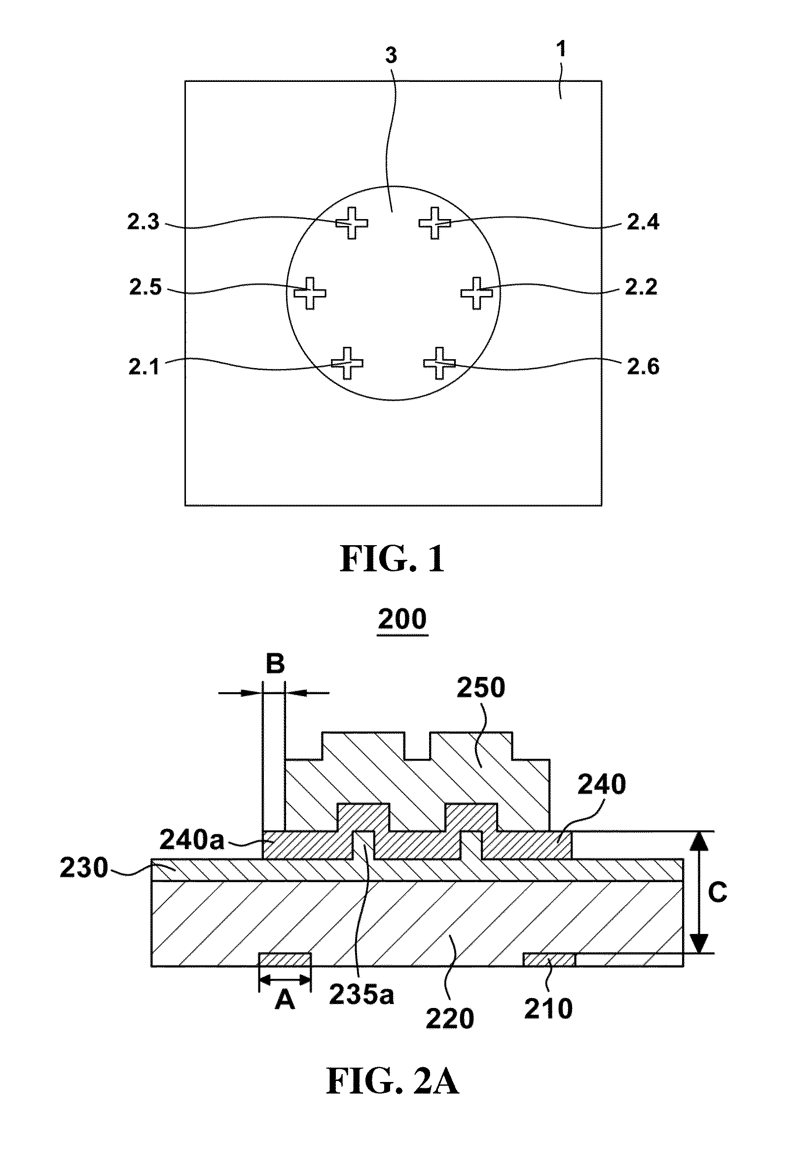
[0051]FIG. 2A is a cross-section view of an example of a magnetic sensor that is formed with a semiconductor substrate.

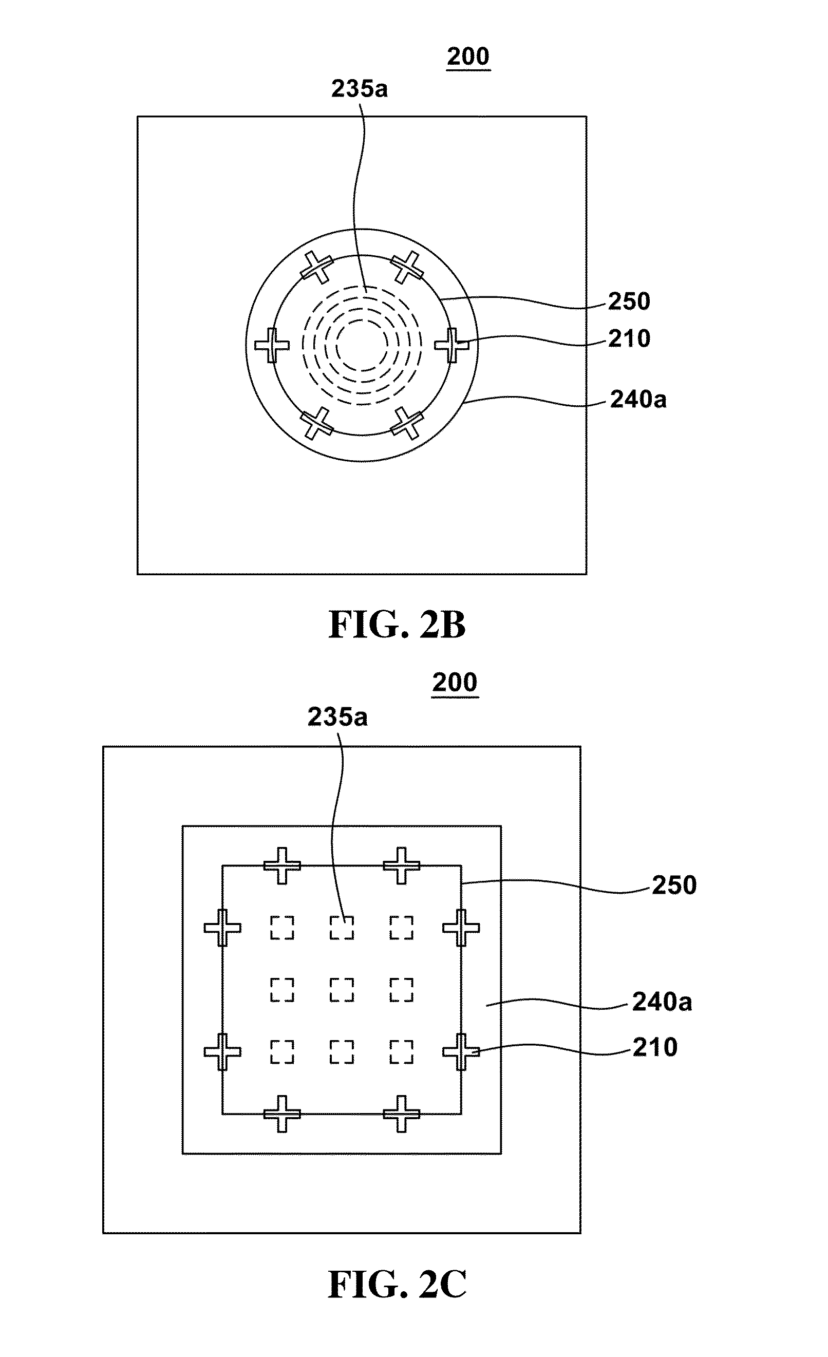
[0052]Referring to FIG. 2A, the magnetic sensor 200 includes a substrate 220 having a plurality of Hall elements 210 arranged therein, a protective layer 230 formed on the substrate 220, a base layer 240 formed on the protective layer 230 and an integrated magnetic concentrator (IMC 250) formed on the base layer 240 and having a bent or an elevated portion on a surface thereof. The substrate 220 may be a s...


PUM


Abstract

A magnetic sensor and a manufacturing method thereof are provided. The magnetic sensor includes: a substrate comprising a plurality of Hall elements, a protective layer formed on the substrate, a base layer formed on the protective layer, and an integrated magnetic concentrator (IMC) formed on the base layer and comprising a surface with an elevated portion. The base layer has a larger cross-sectional area than the IMC.

Description

CROSS-REFERENCE TO RELATED APPLICATIONS[0001]This application claims the benefit under 35 U.S.C. §119(a) of Korean Patent Application No. 10-2013-0066892, filed on Jun. 12, 2013, in the Korean Intellectual Property Office, the entire disclosure of which is incorporated herein by reference for all purposes.BACKGROUND[0002]1. Field[0003]The following description relates to a magnetic sensor and a manufacturing method thereof, and to a semiconductor-based magnetic sensor for digital compass or electronic compass, a semiconductor-based magnetic sensor having Hall elements and integrated magnetic concentrators, and a manufacturing method thereof.[0004]2. Description of Related Art[0005]A semiconductor-based magnetic sensor detects a magnetic signal using a semiconductor device. A semiconductor-based magnetic sensor may include a combination of a plurality of Hall elements and an integrated magnetic concentrator (IMC) that performs magnetic amplification functions.[0006]One type of magnet...

Claims


Application Information

Patent Timeline
Patent Type & Authority Applications(United States)
IPC IPC(8): H01L43/04H01L43/14H10N52/00H10N52/01H10N52/80
CPCH01L43/14H01L43/04G01R33/072G01R33/0011G01R33/0052G01R33/07H10B61/00H10N59/00H10N52/80H10N52/01G01C17/28H10N52/00
Inventor RYU, SEUNG HANJEONG, JONG YEULKIM, KWAN SOO
Owner MAGNACHIP SEMICONDUCTOR LTD
Learn More