Active matrix display, scanning driven circuit and the method thereof

a scanning driven circuit and active matrix technology, applied in the field of active matrix display and scanning driven circuit, can solve the problems of increased bonding difficulty, increased cost, and difficult design of active matrix display, and achieve the effect of reducing the gap between the transmission lines, reducing the number of transmission lines, and reducing the difficulty of bonding

Inactive Publication Date: 2014-12-25
TCL CHINA STAR OPTOELECTRONICS TECH CO LTD
View PDF3 Cites 0 Cited by
  • Summary
  • Abstract
  • Description
  • Claims
  • Application Information

AI Technical Summary

Benefits of technology

[0006]The object of the invention is to provide an active matrix display, the scanning driven circuit and the method thereof to reduce the number of the transmission lines.
[0026]In view of the above, the scanning driven circuit includes a delaying module. An input end of the delaying module receives input signals integrated by initial clock voltage pulse (CKV) signals and start voltage pulse (STV) signals. The input signals are delayed by a first delayed portion and a second delayed portion such that a first output of the delaying module outputs output enable (OE) signals and a second output of the delaying module outputs the delayed CKV signals. The OE signals and the delayed CKV signals are output to scanning lines of the active matrix display. Only one corresponding transmission line is needed to transmit the input signals. The number of the transmission lines is decreased, which contributes to the narrow bezel design. On the other hand, the gap between the transmission lines is increased such that the bonding difficulty is reduced. Furthermore, the number of the output pins of the timing control chips and that of the input pins of the scanning driven chips are decreased such that the cost is reduced.

Problems solved by technology

As such, the design of the active matrix display, especially for the narrow bezel one, is difficult.
It can be understood that while a plurality of transmission lines are arranged on the soft circuit board, the bonding difficulty is increased.
Moreover, a plurality of output pins of corresponding timing control chips and input pins of corresponding scanning driven chips are needed, which result in additional cost.

Method used


Image

  • Active matrix display, scanning driven circuit and the method thereof
  • Active matrix display, scanning driven circuit and the method thereof
  • Active matrix display, scanning driven circuit and the method thereof

Examples


Embodiment Construction

[0036]Embodiments of the invention will now be described more fully hereinafter with reference to the accompanying drawings, in which embodiments of the invention are shown.

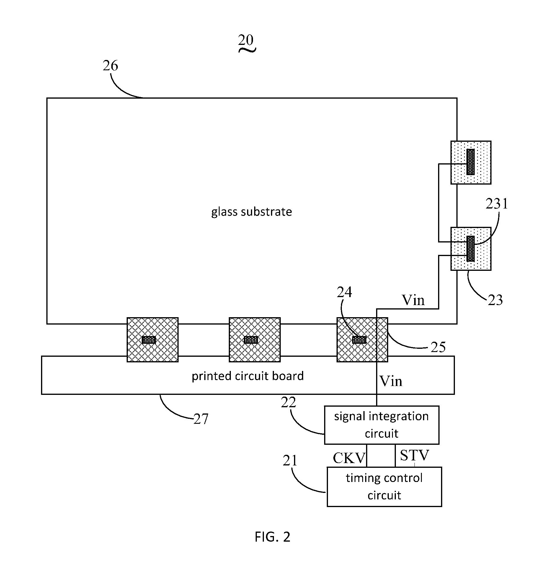
[0037]FIG. 2 is a schematic view of the active matrix display in accordance with one embodiment. The active matrix display 20 includes a timing control circuit 21, a signal integration circuit 22, and a scanning driven circuit 23.

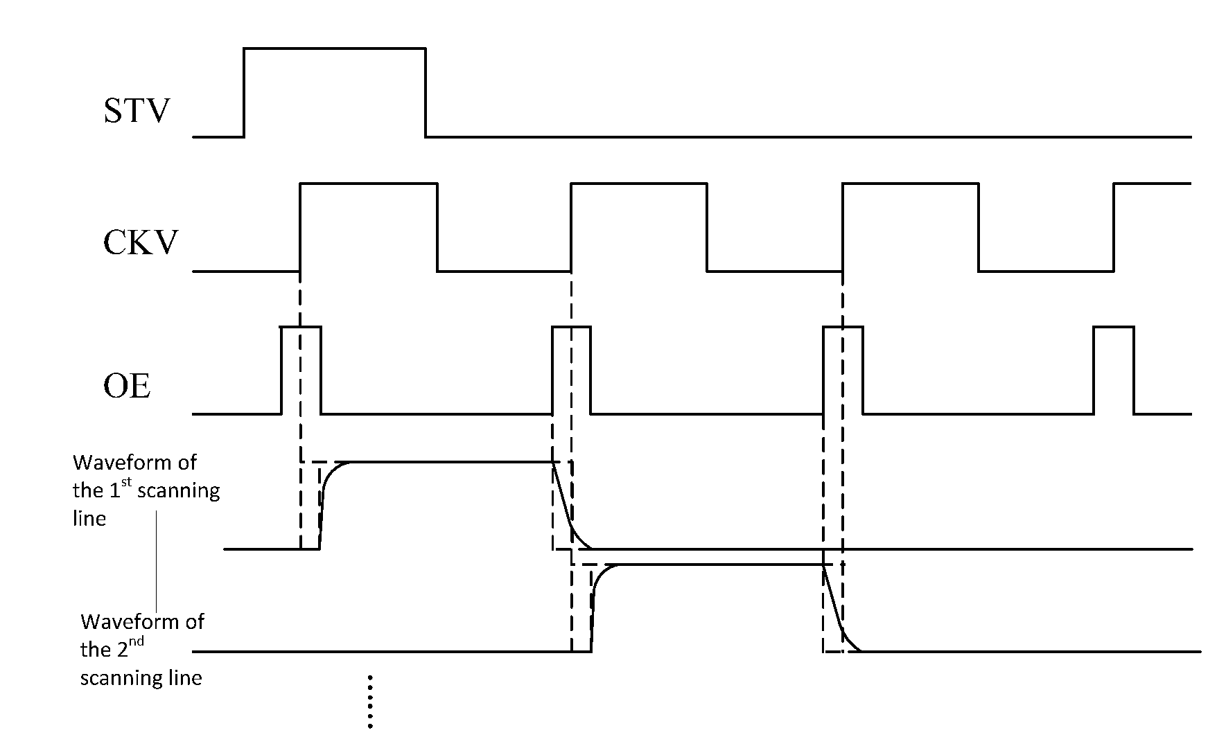
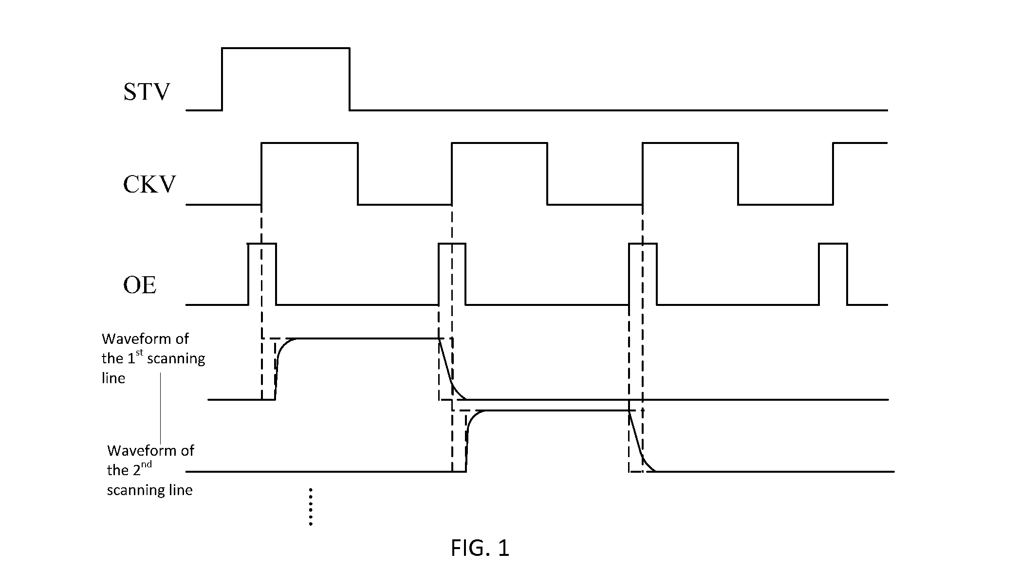
[0038]The timing control circuit 21 generates initial CKV signals and STV signals.

[0039]An input end of the signal integration circuit 22 couples an output end of the timing control circuit 21 to overlap the initial CKV signals and STV signals such that the input signals Vin is generated. FIG. 3 shows the initial CKV signals and STV signals that satisfy one condition in accordance with one embodiment. As shown, the duration of the initial STV signals is t1, the duration of the initial CKV signals is t2, and the time period of the initial CKV signals is T. In one embodiment, t1, t2, and T...


PUM


Abstract

An active matrix display, and the scanning driven circuit and the scanning driven method thereof are disclosed. The scanning driven circuit includes a delaying module. An input end of the delaying module receives input signals integrated by initial clock voltage pulse (CKV) signals and start voltage pulse (STV) signals. The input signals are delayed by a first delayed portion and a second delayed portion such that a first output of the delaying module outputs output enable (OE) signals and a second output of the delaying module outputs the delayed CKV signals. In this way, the number of the transmission lines is decreased, and the number of the output pins of the timing control chips and that of the input pins of the scanning driven chips are also decreased.

Description

BACKGROUND OF THE INVENTION[0001]1. Field of the Invention[0002]The present disclosure relates to liquid crystal display (LCD) technology, and more particularly to an active matrix display and the scanning driven circuit and method thereof[0003]2. Discussion of the Related Art[0004]Currently, scanning driven chips have three control signals for switching the on / off state of each row of the active matrix display. The control signals are respectively start voltage pulse (STV) signals, clock voltage pulse (CKV) signals, and output enable (OE) signals. FIG. 1 is a waveform diagram of conventional scanning driven signals. As shown, the STV signals control the initial state of the first row. The CKV signals control the on / off frequency of each row. Upon detecting the rising edge of the STV signals, the OE signals are arranged between the on and off state of each rows. The OE signals compress the output voltage during the high level period. The OE signals control the switching time of the ...

Claims


Application Information

Patent Timeline
Patent Type & Authority Applications(United States)
IPC IPC(8): G09G5/18
CPCG09G5/18G09G3/3688G09G2370/08G09G3/3677
Inventor GUO, DONGSHENGQIN, HONGJIANG
Owner TCL CHINA STAR OPTOELECTRONICS TECH CO LTD
Why Eureka
Try Eureka