Semiconductor device integrating a voltage divider and process for manufacturing a semiconductor device

a technology of semiconductor devices and voltage dividers, which is applied in the direction of solid-state devices, transistors, basic electric elements, etc., can solve the problems of increasing the resistivity, and affecting the performance of the devi

Active Publication Date: 2015-01-01
STMICROELECTRONICS INT NV
View PDF8 Cites 68 Cited by
  • Summary
  • Abstract
  • Description
  • Claims
  • Application Information

AI Technical Summary

Benefits of technology

[0013]According to an embodiment, there is provided a semiconductor device comprising a semiconductor substrate; a high-voltage first resistive structure extending along a spiral path above the substrate and separated from the substrate by a first dielect

Problems solved by technology

Resistors of this type exploit very well the available area and do not present corners, which could easily lead to conditions of breakdown, given the voltages involved.
However, known high-voltage resistors suffer from some limitations.
The voltage differences that are created cause depletion regions at the interface of the polysilicon forming the resistors and reduce the conduction section, increasing the resistivity.
This solution has proven ef

Method used


Image

  • Semiconductor device integrating a voltage divider and process for manufacturing a semiconductor device
  • Semiconductor device integrating a voltage divider and process for manufacturing a semiconductor device
  • Semiconductor device integrating a voltage divider and process for manufacturing a semiconductor device

Examples


Embodiment Construction

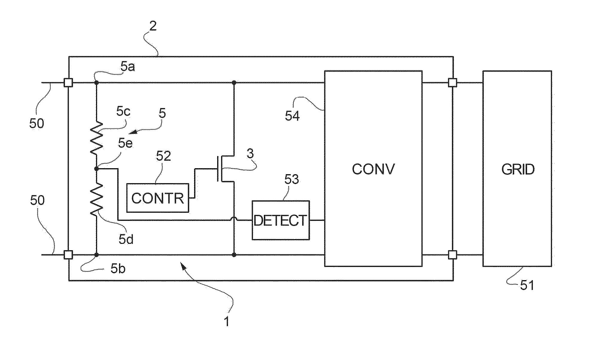
[0042]In FIG. 1, reference number 1 designates a semiconductor device made in a chip 2. In one embodiment, the semiconductor device 1 may comprise or be incorporated in a power supply or a battery charger for a portable electronic device, such as a cellphone, a tablet, a portable computer, a video camera, a photographic camera, a console for videogames, and so on. In particular, FIG. 1 also shows an electrical supply line 50, for example supplying a 220-V, 50-Hz or 110-V, 60-Hz a.c. voltage, and an electronic apparatus 51 supplied through the semiconductor device 1. It is in any case understood that the embodiments may advantageously be used also for applications and in environments different from what has been mentioned above, in all the cases where it is necessary to use a resistive power component.

[0043]The semiconductor device 1 comprises an active power component, in particular a MOS transistor 3, and a high-voltage resistive structure 5, which are incorporated in the chip 2. T...


PUM


Abstract

A semiconductor device includes: a semiconductor substrate; a high-voltage first resistive structure which extends along a spiral path above the substrate and is separated from the substrate by a first dielectric layer; and a conductive shielding structure, including a plurality of first shielding strips, which are arranged in sequence along respective portions of the first resistive structure and are separated from the first resistive structure by a second dielectric layer.

Description

CROSS REFERENCE TO RELATED APPLICATIONS[0001]This application claims the priority benefit of Italian Patent Application No. TO2013A000541, filed Jun. 28, 2013, and which application is hereby incorporated by reference to the maximum extent allowable by law.BACKGROUND[0002]1. Technical Field[0003]The present disclosure relates to a semiconductor device integrating a voltage divider and to a process for manufacturing a semiconductor device.[0004]2. Discussion of the Related Art[0005]Known to the art are particular types of semiconductor devices integrating resistors for medium-to-high voltage applications, which are capable of withstanding voltages on the order of some hundreds of volts or even higher.[0006]For example, in power supplies and / or battery chargers of many portable electronic devices, semiconductor voltage dividers are used for detecting the grid voltage, as well as for performing further functions. In these cases, the resistors should withstand voltages of 500-800 V.[000...

Claims


Application Information

Patent Timeline
IPC IPC(8): H01L49/02
CPCH01L28/20G01R15/04H01L23/5225H01L23/5228H01L23/585H01L27/0207H01L27/0629H01L29/0692H01L29/1033H01L29/405H01L2924/0002H01L29/0696H01L29/1095H01L29/66681H01L29/7817
Inventor PALUMBO, VINCENZOVENTURATO, MIRKO
Owner STMICROELECTRONICS INT NV
Why Eureka
Try Eureka