Supercharge Your Innovation With Domain-Expert AI Agents!

Using an integrated circuit die configuration for package height reduction

Active Publication Date: 2015-01-08
NXP USA INC
View PDF5 Cites 9 Cited by
  • Summary
  • Abstract
  • Description
  • Claims
  • Application Information

AI Technical Summary

Benefits of technology

The patent text discusses the challenges in reducing the size of semiconductor devices while addressing issues such as heat dissipation and ensuring reliable functioning. The invention provides a solution by incorporating a notch in the semiconductor die to allow for a lead frame to fit in and reducing the thickness of the die while maintaining its strength. The text also describes different configurations and methods for forming the notch. The technical effect of this invention is to allow for a smaller final package size while addressing the challenges of reducing the size of semiconductor devices.

Problems solved by technology

Each of these elements must maintain their intended function reliably which can be difficult.
Another continuing issue is heat dissipation.
One difficulty with heat dissipation is the ability to directly access the die, which is the source of the heat.
Packages that allow this, such as lead-on-chip, raise more difficult manufacturing issues than the more conventional approach of bonding a die to a metal flag.

Method used


Image

  • Using an integrated circuit die configuration for package height reduction
  • Using an integrated circuit die configuration for package height reduction
  • Using an integrated circuit die configuration for package height reduction

Examples


Embodiment Construction

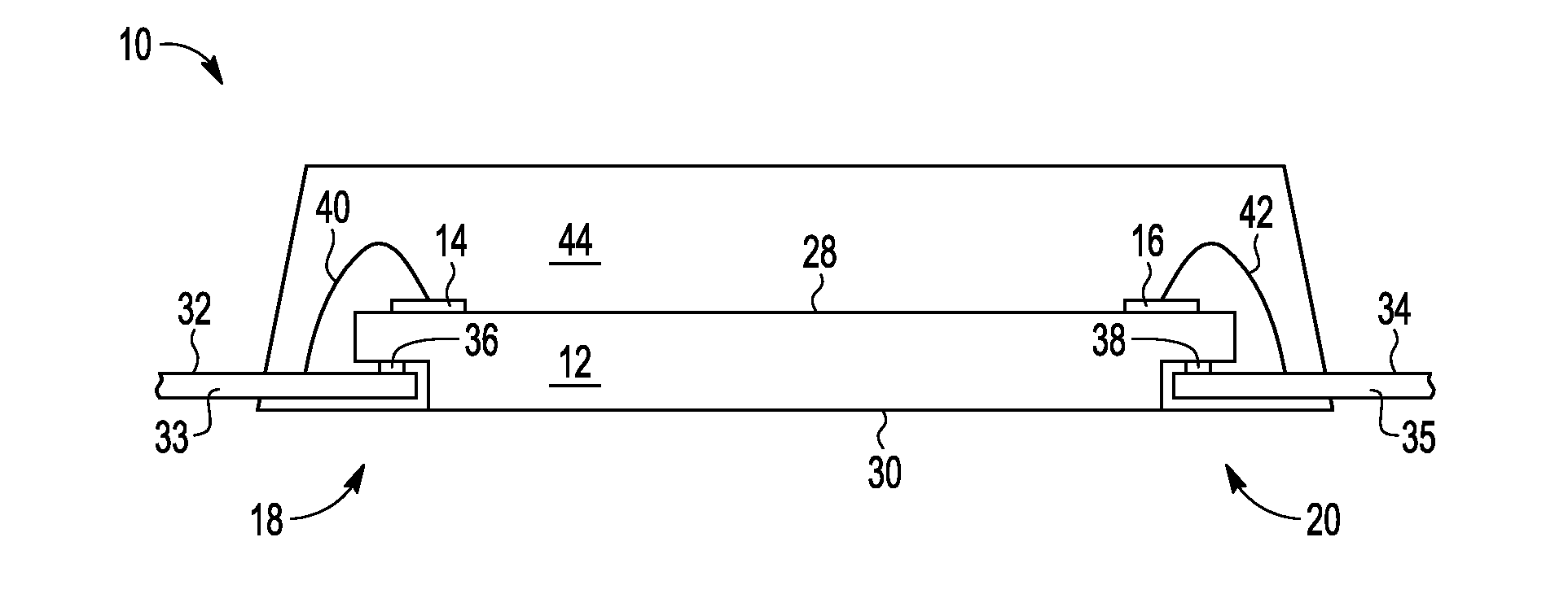
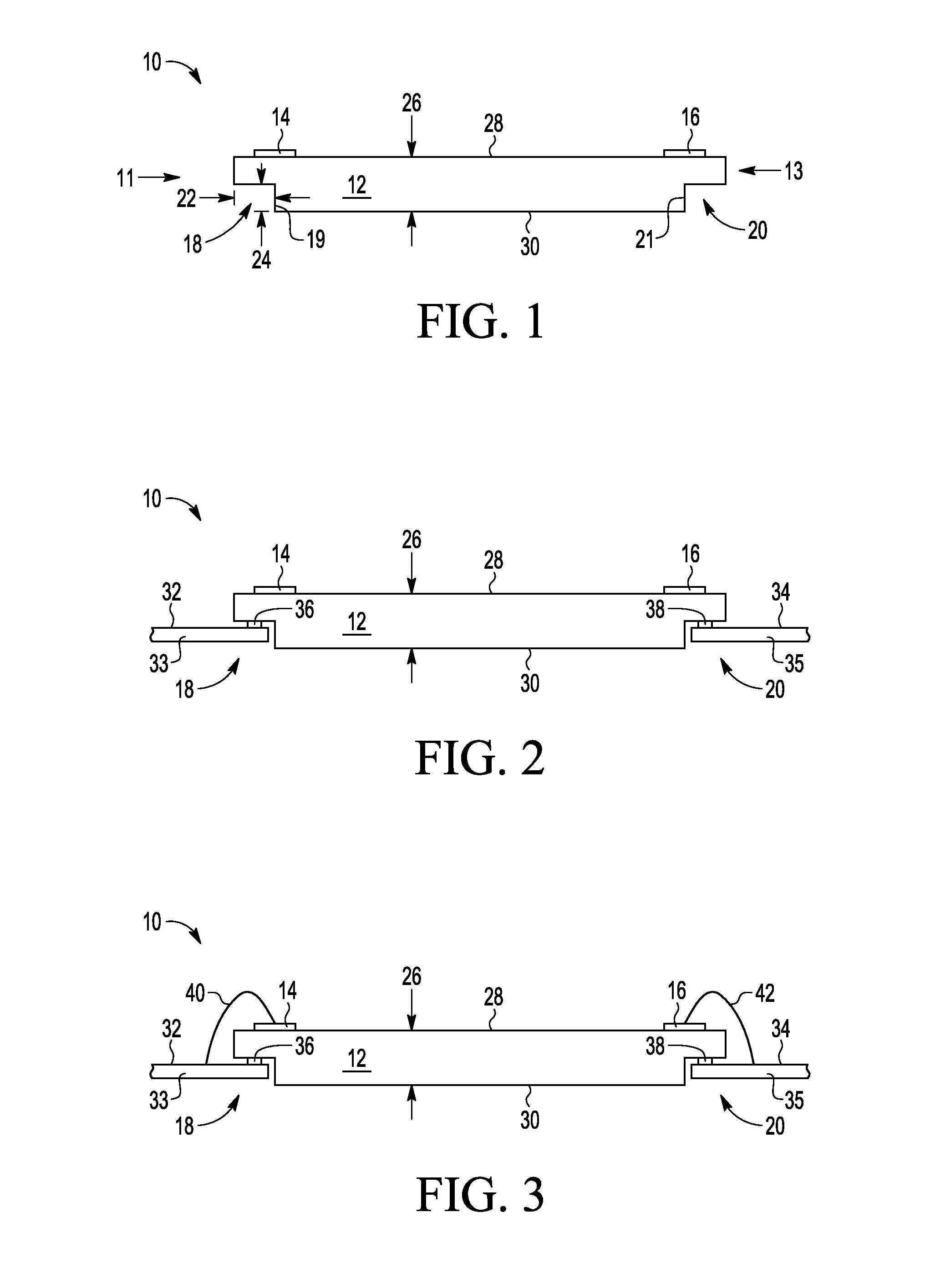
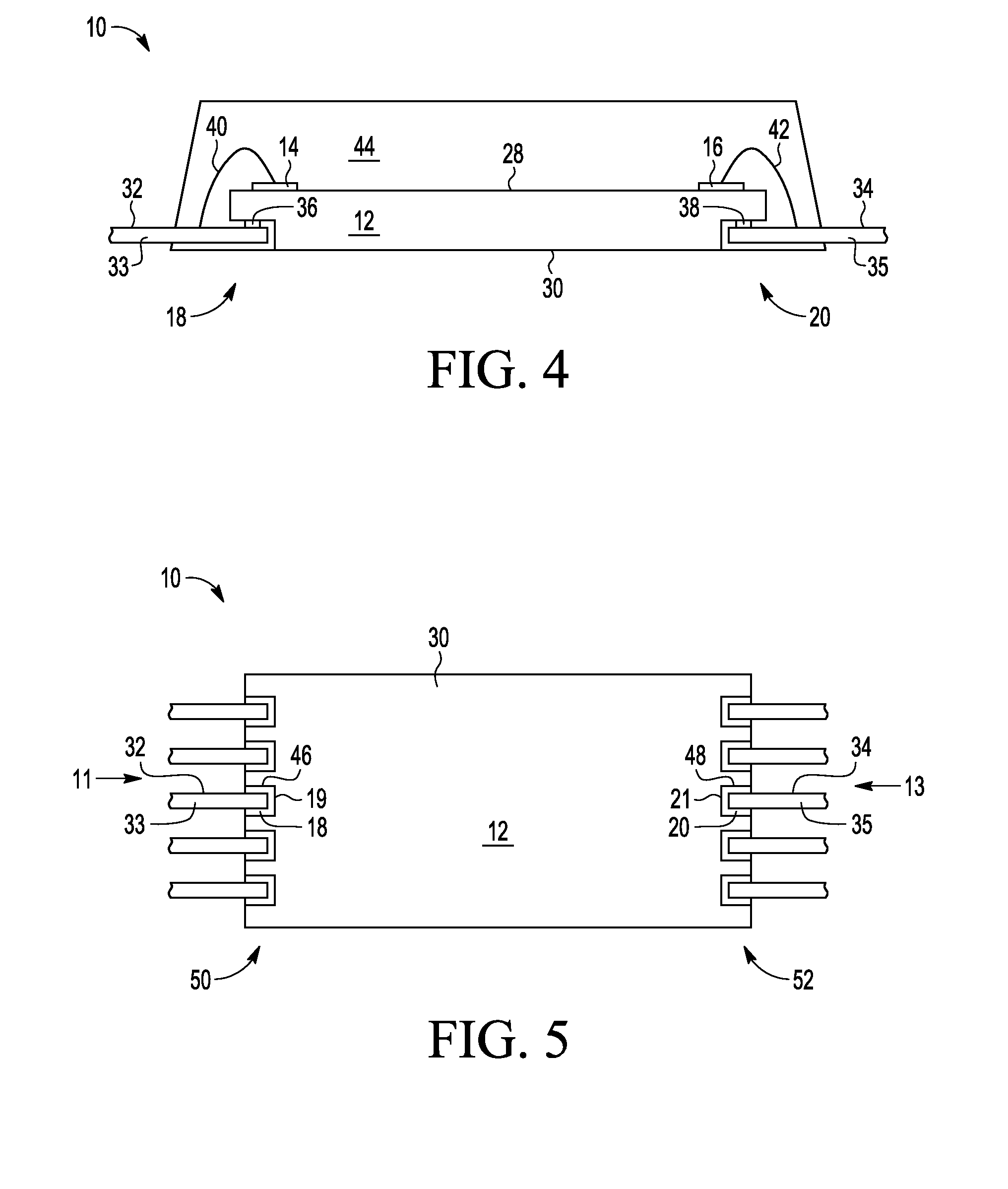
[0016]In one aspect, a semiconductor device includes a semiconductor die having a bottom edge with a notch that allows a lead of a lead frame to fit in the notch. This reduces the increase in height that occurs when a lead frame is placed under the semiconductor device. This is better understood by reference to the drawings and the following description.

[0017]Shown in FIG. 1 is a semiconductor device 10 having a semiconductor die 12 having an active side 28 and a backside 30, which are the major surfaces 28 and 30 of semiconductor die 12. Die 12 may include a plurality of substrate layers. Active side 28 is also the top side in this example. Semiconductor die 12 has contact pads 14 and 16 on active side 28, a notch 18 along a first edge 11 of backside 30, and a notch 20 along a second edge 13 of backside 30. The first and second edges 11 and 13 may be considered minor surfaces 11 and 13 of semiconductor die 12. Notch 18 may be one a plurality of notches along the first edge in one c...


PUM


Abstract

A semiconductor device includes a semiconductor die having a first major surface and a second major surface opposite the first major surface, a first minor surface and a second minor surface opposite the first minor surface, a plurality of contact pads on the first major surface, and a notch which extends from the first minor surface and the second major surface into the semiconductor die. The notch has a notch depth measured from the second major surface into the semiconductor die, wherein the notch depth is less than a thickness of the semiconductor die, and a notch length measured from the first minor surface into the semiconductor die, wherein the notch length is less than a length of the semiconductor die measured between the first and second minor surfaces. The device includes a lead having a first end in the notch, and an encapsulant over the first major surface.

Description

BACKGROUND[0001]1. Field[0002]This disclosure relates generally to packaging integrated circuits, and more specifically, to die configurations of the integrated circuits that are useful in packaging.[0003]2. Related Art[0004]In the field of semiconductors, a continuing goal is to reduce dimensions and this includes the dimensions of the final package. The total area is important but also the height of the packaged device. The height can be reduced by thinning the various elements that determine device height such as the thickness of the die, the thickness of the supporting package, the height of wire bonds, and the thickness of the encapsulant. Each of these elements must maintain their intended function reliably which can be difficult. Die thickness relates to sufficient strength to be moved in wafer form. The encapsulant must provide sufficient protection for the die. The height of the wire bonds must be sufficient to be reliable and avoid shorting. The supporting package must be ...

Claims


Application Information

Patent Timeline
IPC IPC(8): H01L23/495H01L23/31H01L23/00
CPCH01L23/4951H01L24/97H01L23/3114H01L29/0657H01L2224/32014H01L2224/32052H01L2224/32245H01L2224/48247H01L2224/73265H01L2924/18165H01L23/3107H01L24/48H01L2224/48091H01L2224/73257H01L2924/00014H01L2924/10155H01L2924/181H01L2924/12042H01L24/73H01L2224/16245H01L2224/97H01L2924/10158H01L2224/0401H01L2224/04042H01L2224/05571H01L2224/06181H01L24/16H01L2224/48245H01L2924/00012H01L2224/45099H01L2924/00H01L2224/45015H01L2924/207H01L2224/05599
Inventor PHAM, TIM V.GUAJARDO, JAMES R.MCSHANE, MICHAEL B.
Owner NXP USA INC
Features
  • R&D
  • Intellectual Property
  • Life Sciences
  • Materials
  • Tech Scout
  • Unparalleled Data Quality
  • Higher Quality Content
  • 60% Fewer Hallucinations
Learn More