

Electronic component embedded substrate and method for manufacturing electronic component embedded substrate
- Summary
- Abstract
- Description
- Claims
- Application Information
AI Technical Summary
Benefits of technology
Problems solved by technology
Method used
Image

Examples
Embodiment Construction
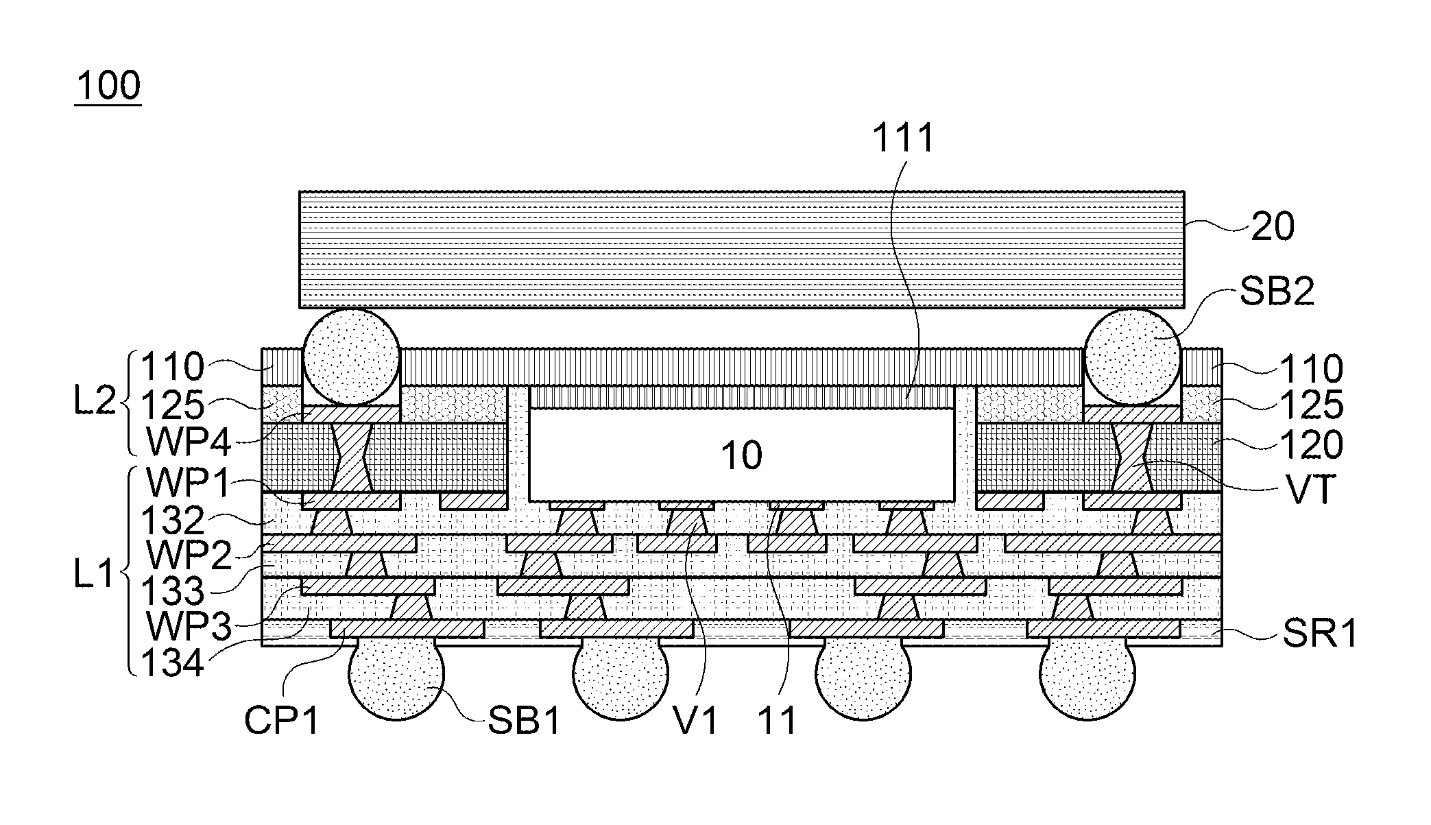
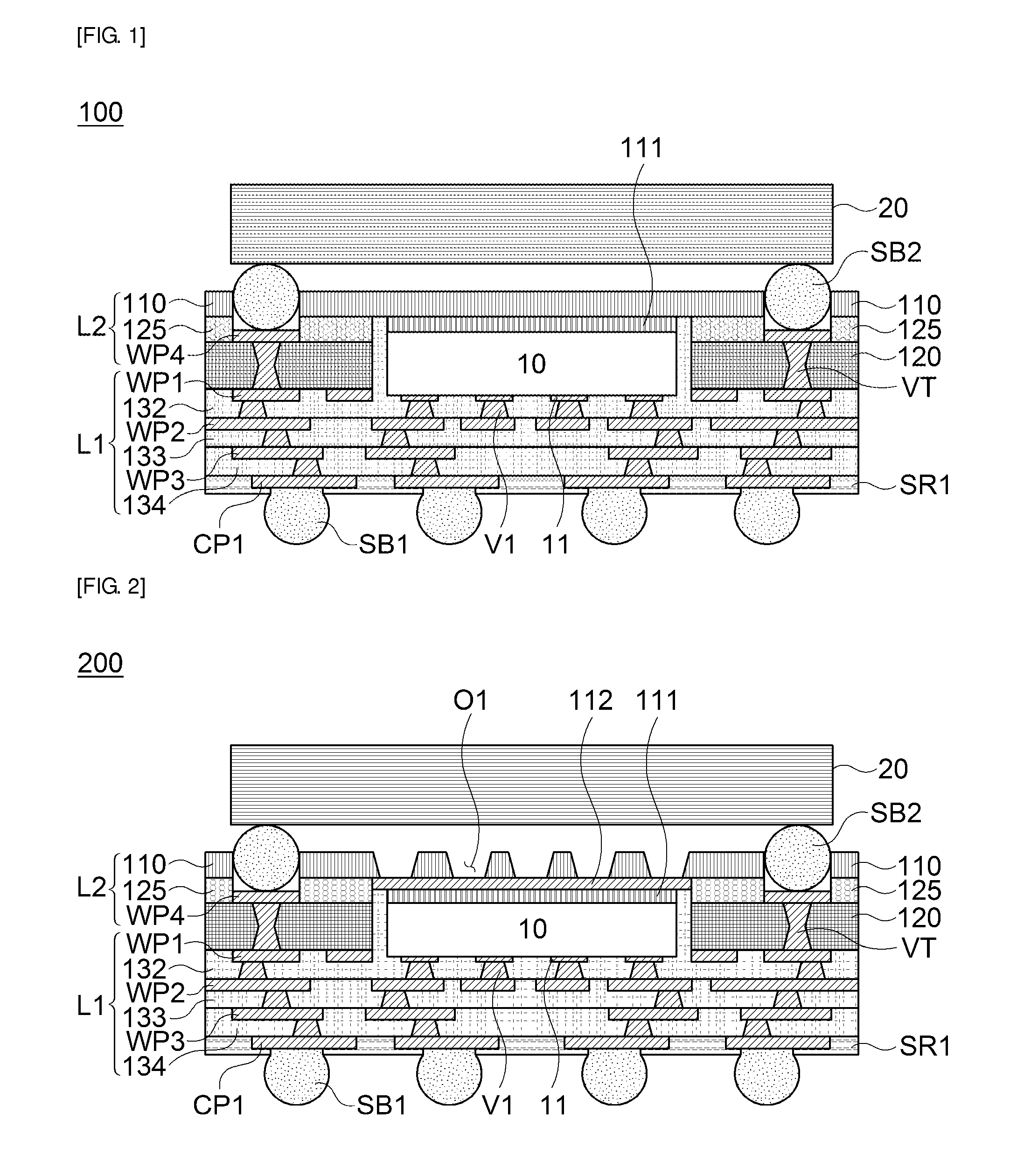
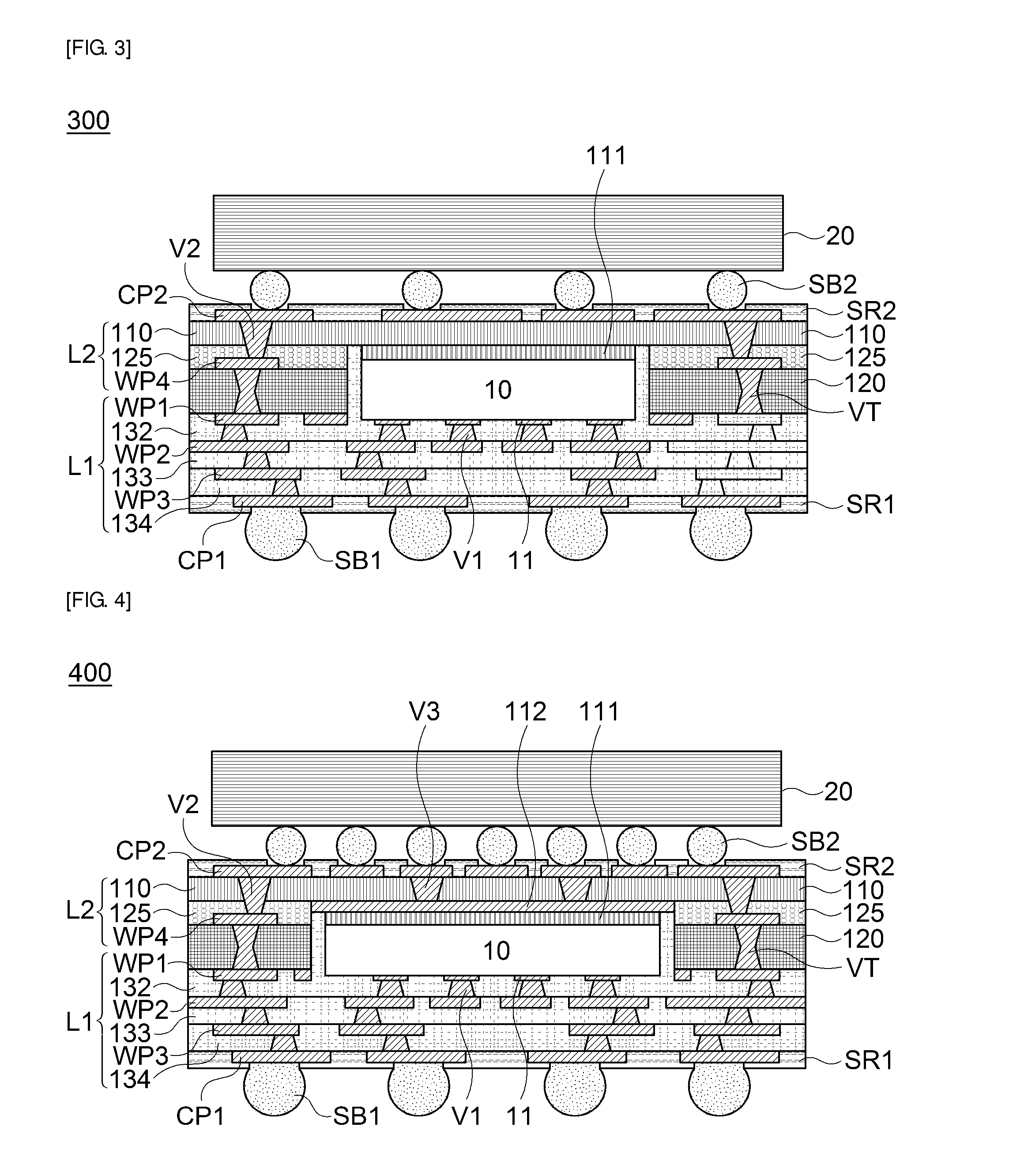
[0058]Advantages and features of the present invention and methods of accomplishing the same will be apparent by referring to embodiments described below in detail in connection with the accompanying drawings. However, the present invention is not limited to the embodiments disclosed below and may be implemented in various different forms. The embodiments are provided only for completing the disclosure of the present invention and for fully representing the scope of the present invention to those skilled in the art. Like reference numerals refer to like elements throughout the specification.
[0059]Terms used herein are provided to explain embodiments, not limiting the present invention. Throughout this specification, the singular form includes the plural form unless the context clearly indicates otherwise. When terms “comprises” and / or “comprising” used herein do not preclude existence and addition of another component, step, operation and / or device, in addition to the above-mentione...
PUM
| Property | Measurement | Unit |
|---|---|---|
| Time | aaaaa | aaaaa |
| Density | aaaaa | aaaaa |
| Coefficient of linear thermal expansion | aaaaa | aaaaa |
Abstract
Description
Claims
Application Information