
Eureka
For R&D, Eureka makes reading and utilizing patents & technical documents easy.
Eureka AIR
Designed for self-driven R&D workflows. Generate viable solutions, solve complex R&D challenges, empower your innovation with AI.

Eureka Materials
Designed for material experts only. Revolutionize your material R&D, from search, analyze, to developing new materials.

TechResearch
Generate reliable direction feasibility study reports for your R&D in just a few steps.

TechSeek
Discover and master advanced knowledge NOW. Basics, ideas, possibilities, all at once.

TechMind
As an expert in R&D Theories, TechMind can generates customized viable solutions instantly.

TechRisk
Analyze your overall solution with one click, know your potential R&D risks in advance.

TechMonitor
Get weekly tech updates, stay abreast of the latest tech innovations and key insights.
Group iii nitride semiconductor light-emitting device
a semiconductor light-emitting device and semiconductor light-emitting technology, which is applied in the direction of semiconductor devices, electrical equipment, basic electric elements, etc., can solve the problems of insufficient improvement of light extraction performance of light-emitting devices, and achieve the effect of improving light extraction performan
- Summary
- Abstract
- Description
- Claims
- Application Information
AI Technical Summary
Benefits of technology
Problems solved by technology
Method used
Image

Examples
embodiment 1
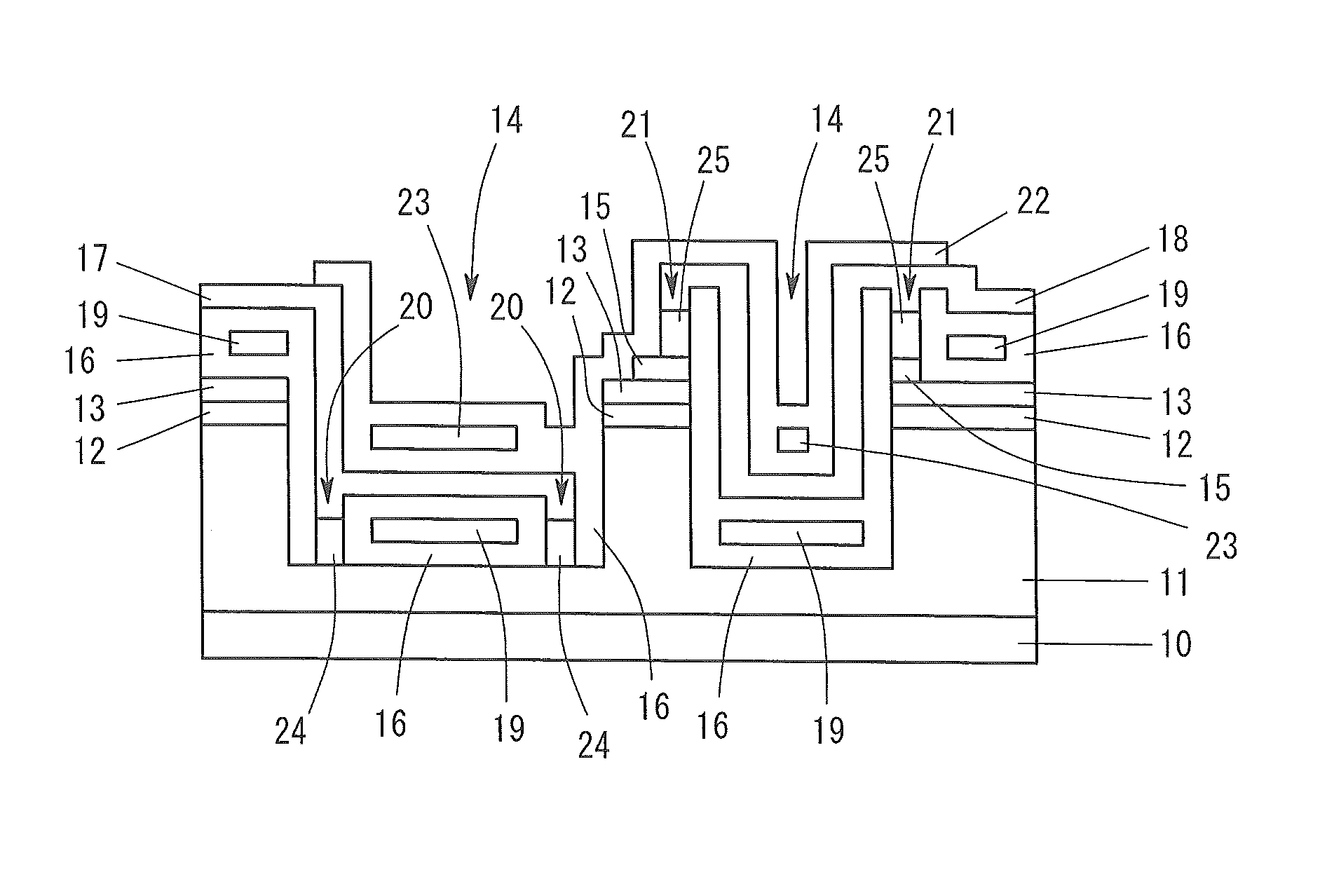
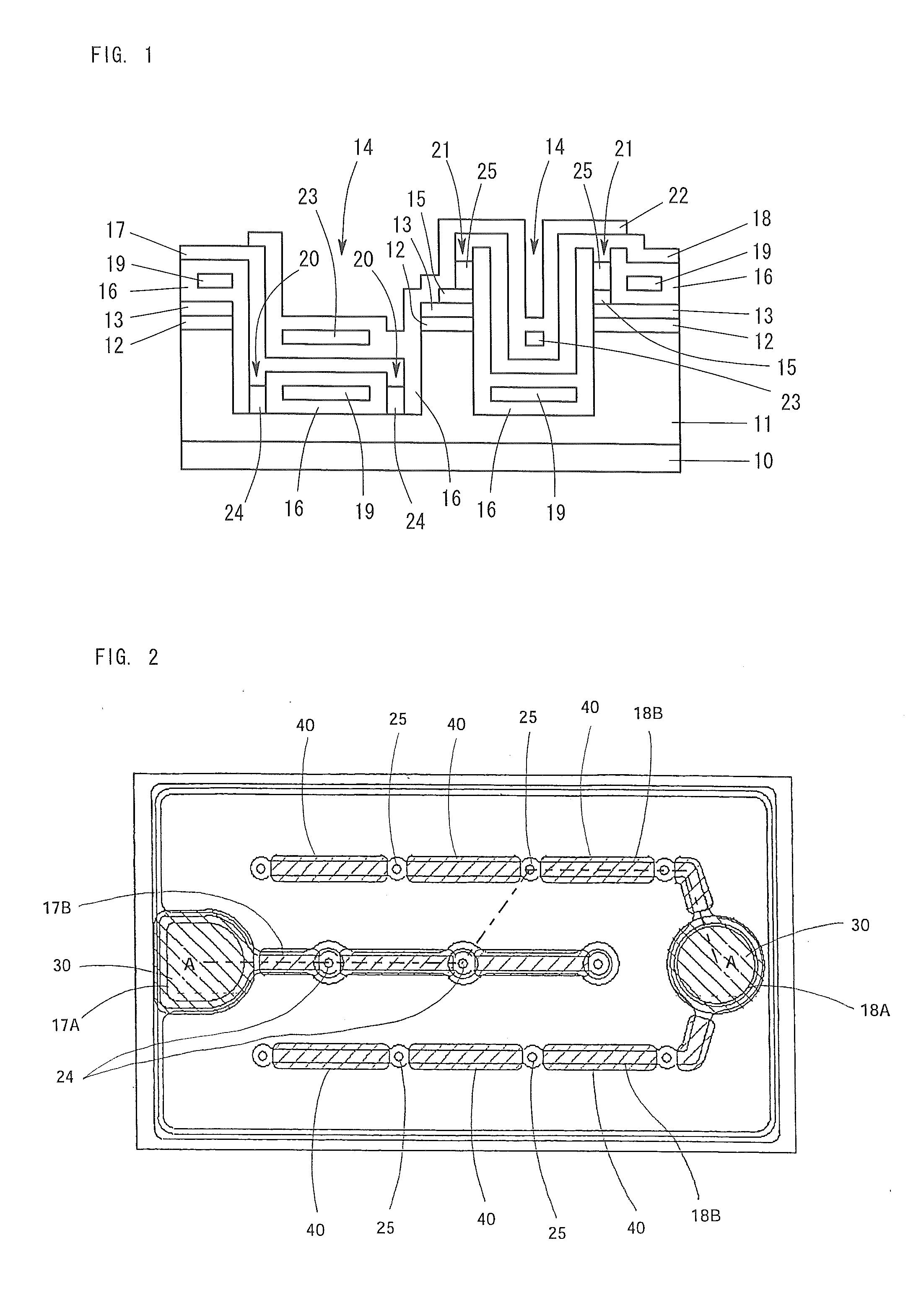
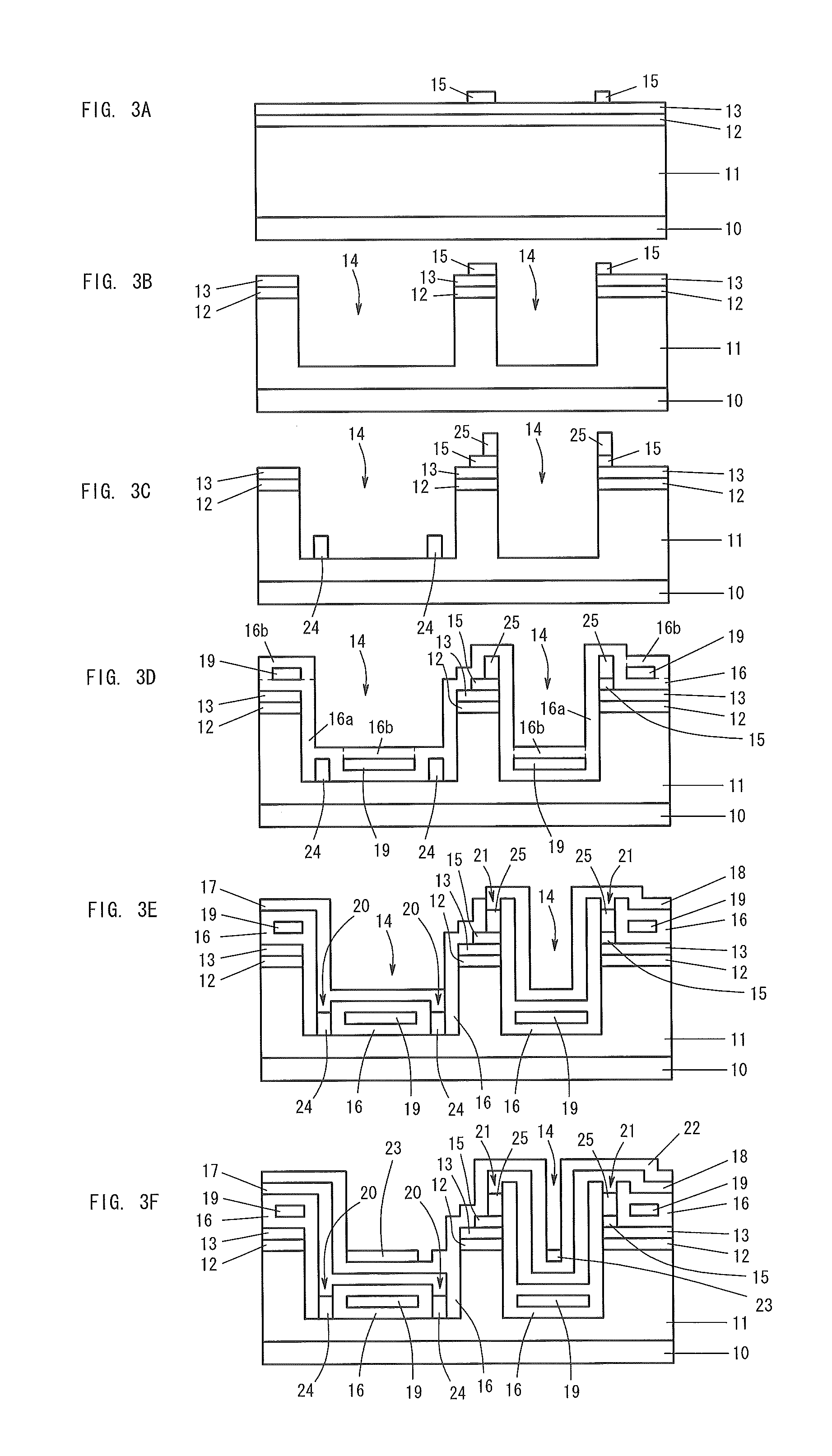
[0056]FIG. 1 shows the configuration of a face-up-type Group III nitride semiconductor light-emitting device according to Embodiment 1. FIG. 2 is a top view of the Group III nitride semiconductor light-emitting device according to Embodiment 1. FIG. 1 corresponds to a cross section taken along line A-A of FIG. 2.
[0057]As shown in FIG. 2, the Group III nitride semiconductor light-emitting device according to Embodiment 1 has a rectangular shape in plan view, and includes an n-electrode 17 and a p-electrode 18. The n-electrode 17 has a bonding portion 17A, and a wiring portion 17B continuous with the bonding portion 17A. Also, the p-electrode 18 has a bonding portion 18A and a wiring portion 18B. The bonding portion 17A or 18A is a region to which a bonding wire is connected, and voltage is applied to the n-electrode 17 or the p-electrode 18 by means of the bonding wire. The wiring portion 17B or 18B has a linear structure extending in a direction parallel to the main surface of the d...
embodiment 2
[0074]FIG. 4 is a cross-sectional view of the configuration of a face-up-type Group III nitride semiconductor light-emitting device according to Embodiment 2. The Group III nitride semiconductor light-emitting device according to Embodiment 2 has the same configuration as the Group III nitride semiconductor light-emitting device according to Embodiment 1, except that the reflective films 19 are replaced with reflective films 119 which are provided directly on the n-type layer 11 and on the p-type layer 13 (without the mediation of the insulating film 16). Similar to the case of the reflective films 19, the reflective films 119 are provided directly below the wiring portion 17B of the n-electrode 17 and the wiring portion 18B of the p-electrode 18 by the mediation of the insulating film 16, and are located at a level lower than that of the light-emitting layer 12.
[0075]Similar to the case of Embodiment 1, the Group III nitride semiconductor light-emitting device according to Embodime...
embodiment 3
[0078]FIG. 5 is a cross-sectional view of the configuration of a face-up-type Group III nitride semiconductor light-emitting device according to Embodiment 3. The Group III nitride semiconductor light-emitting device according to Embodiment 3 has the same configuration as the Group III nitride semiconductor light-emitting device according to Embodiment 1, except that the reflective films 19 are omitted.
[0079]Similar to the case of Embodiment 1, the Group III nitride semiconductor light-emitting device according to Embodiment 3 exhibits improved light extraction performance. The reasons for this are as follows. The reflective films 23 in regions directly above the wiring portion 17B of the n-electrode 17 and the wiring portion 18B of the p-electrode 18 are located at a level lower than that of the light-emitting layer 12. Therefore, light reflected by the reflective films 23 is less likely to be directed toward the light-emitting layer 12, and absorption of light by the light-emittin...
PUM
 Abstract
Description
Claims
Application Information
 - R&D Engineer
- R&D Manager
- IP Professional
- Industry Leading Data Capabilities
- Powerful AI technology
- Patent DNA Extraction
Browse by: Latest US Patents, China's latest patents, Technical Efficacy Thesaurus, Application Domain, Technology Topic, Popular Technical Reports.
© 2024 PatSnap. All rights reserved.Legal|Privacy policy|Modern Slavery Act Transparency Statement|Sitemap|About US| Contact US: help@patsnap.com