Eureka AIR delivers breakthrough ideas for toughest innovation challenges, trusted by R&D personnel around the world.

Group iii nitride semiconductor light-emitting device and production method therefor

Inactive Publication Date: 2012-05-24
TOYODA GOSEI CO LTD
View PDF3 Cites 16 Cited by
  • Summary
  • Abstract
  • Description
  • Claims
  • Application Information

AI Technical Summary

Benefits of technology

[0008]In view of the foregoing, an object of the present invention is to realize a Group III nitride semiconductor light-emitting device exhibiting further improved light extraction performance.
[0013]Other examples of the structure of the embossment of the substrate are as follows. For example, the embossment of the substrate may have a structure including a stripe-pattern embossment, and a dot-pattern embossment provided atop the stripe-pattern embossment, wherein the dot-pattern embossment includes a plurality of dents or mesas which are arranged in a grid pattern. Dents or mesas of the dot-pattern embossment may have, for example, a truncated pyramidal, truncated conical, prismatic, cylindrical, pyramidal, conical, or hemispherical shape. Dents or mesas of the dot-pattern embossment may be arranged in a grid pattern (e.g., quadrangular or triangular grid pattern). Alternatively, the embossment of the substrate may have a structure including a dot-pattern embossment and a stripe-pattern embossment provided atop the dot-pattern embossment, wherein the dot-pattern embossment includes a plurality of dents or mesas which are arranged in a grid pattern. Side surfaces of dents (or mesas) of the dot-pattern embossment are preferably inclined by 40° to 80° with respect to the main surface of the sapphire substrate. When the angle falls within the above range, light extraction performance can be further improved.
[0018]According to the present invention, since the embossment of the sapphire substrate exhibits the effect of reflecting light propagated in any direction in the device, light extraction performance can be further improved.

Problems solved by technology

However, when a stripe-pattern embossment is formed on a sapphire substrate, since no difference in level is provided in the direction of the stripe, light propagated along the stripe may fail to be reflected or scattered upward, resulting in insufficient improvement of light extraction performance.
Therefore, in some regions of the substrate, no difference in level is provided in a specific direction, resulting in insufficient improvement of light extraction performance.

Method used


Image

  • Group iii nitride semiconductor light-emitting device and production method therefor
  • Group iii nitride semiconductor light-emitting device and production method therefor
  • Group iii nitride semiconductor light-emitting device and production method therefor

Examples


embodiment 1

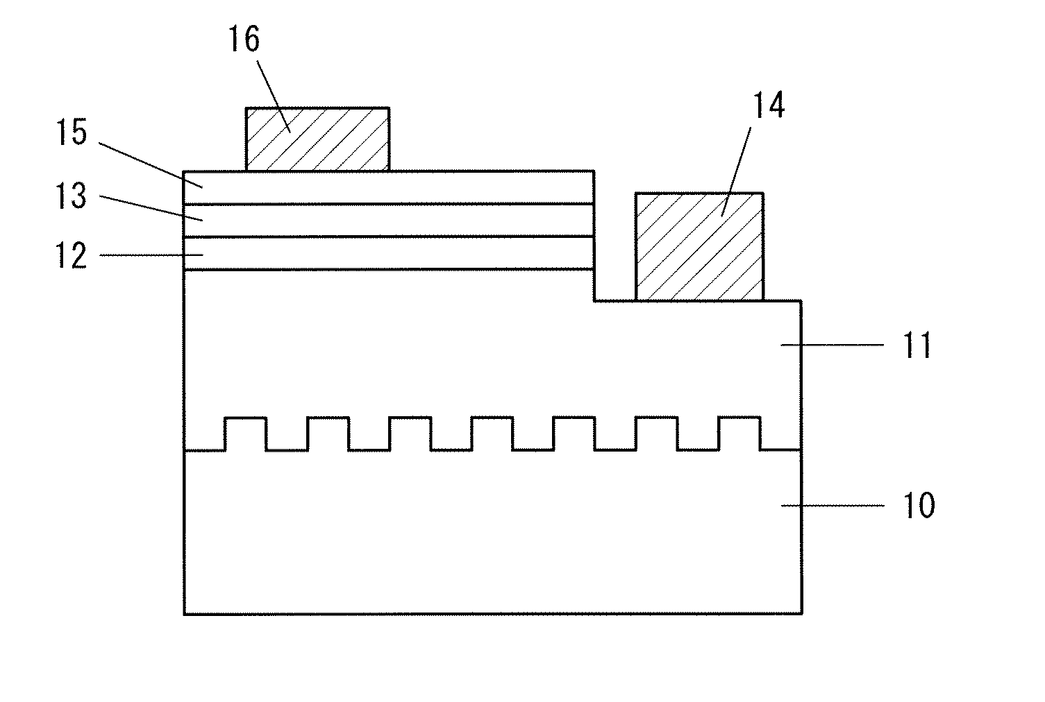
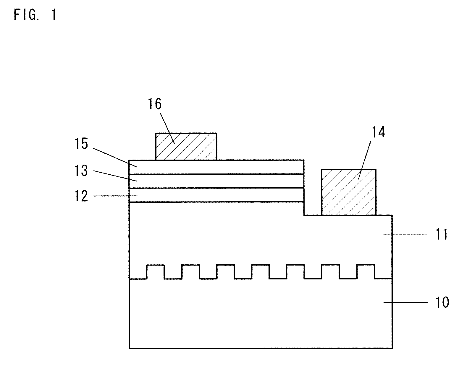
[0026]FIG. 1 shows the configuration of a Group III nitride semiconductor light-emitting device according to Embodiment 1. The Group III nitride semiconductor light-emitting device according to Embodiment 1 includes a sapphire substrate 10 having an embossment on a surface thereof; and an n-type layer 11, a light-emitting layer 12, and a p-type layer 13, which are sequentially deposited on the embossed surface of the sapphire substrate 10 via a buffer layer (not illustrated), and each of which is formed of a Group III nitride semiconductor. The layered structure of the present invention corresponds to a structure including the n-type layer 11, the light-emitting layer 12, and the p-type layer 13. A portion of the light-emitting layer 12 and a portion of the p-type layer 13 are removed, and the corresponding portion of the surface of the n-type layer 11 is exposed. An n-electrode 14 is formed on the exposed portion of the surface of the n-type layer 11. An ITO transparent electrode 1...

example 1-1

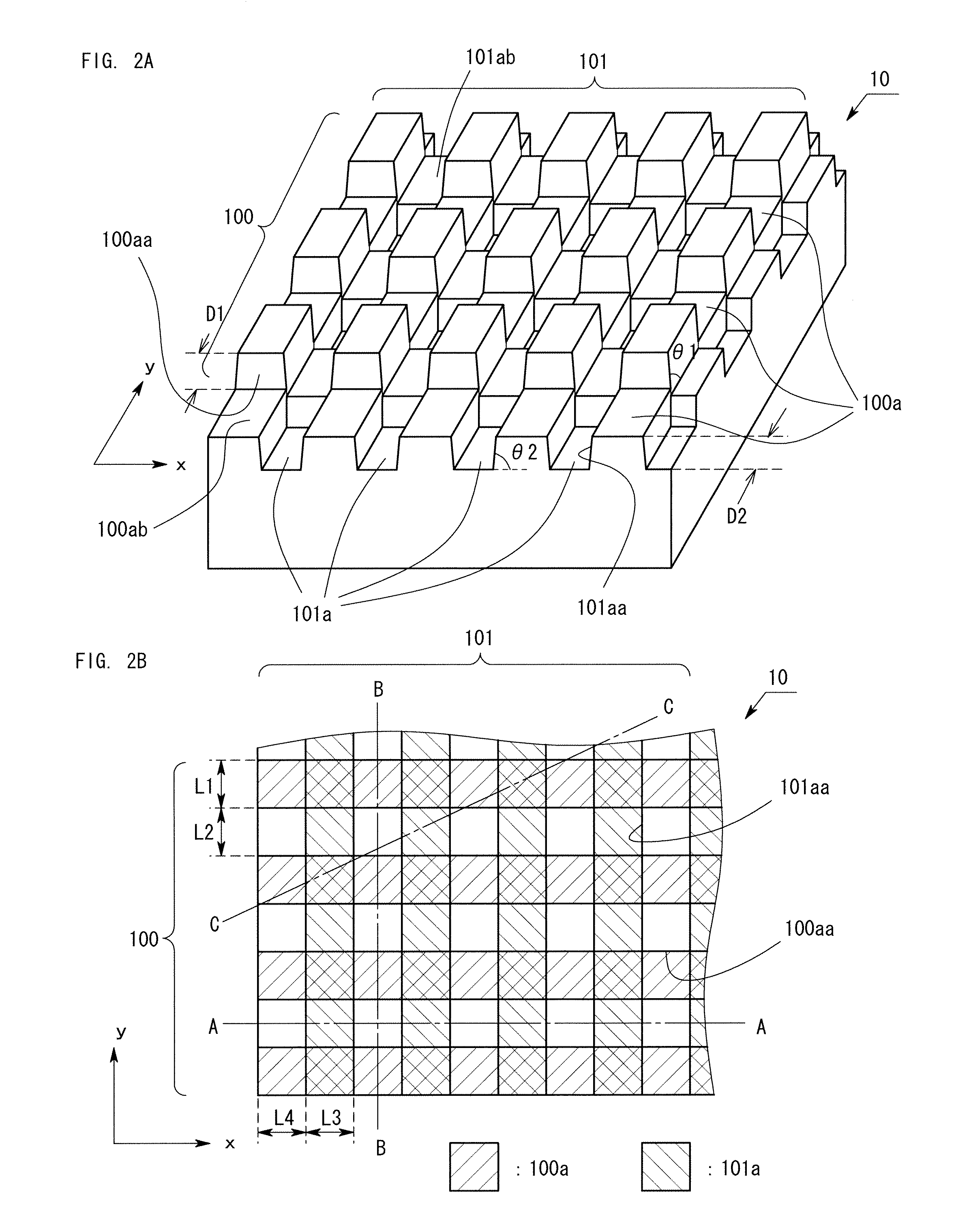
[0042]The width L1, distance L2, and depth D1 of each first groove 100a were adjusted to 2 μm, 2 μm, and 0.7 μm, respectively; the angle θ1 of each side surface 100aa was adjusted to 80°; the width L3, distance L4, and depth D2 of each second groove 101a were adjusted to 1.5 μm, 1.5 μm, and 0.7 μm, respectively; and the angle θ2 of each side surface 101aa was adjusted to 80°. The axial light output of the thus-produced device was measured and found to be 1.19 times that of the device of Comparative Example 1.

example 1-2

[0043]The width L1, distance L2, and depth Dl of each first groove 100a were adjusted to 1.5 μm, 1.5 μm, and 0.7 μm, respectively; the angle θ1 of each side surface 100aa was adjusted to 80°; the width L3, distance L4, and depth D2 of each second groove 101a were adjusted to 1.5 μm, 1.5 μm, and 0.7 μm, respectively; and the angle θ2 of each side surface 101aa was adjusted to 80°. The axial light output of the thus-produced device was measured and found to be 1.17 times that of the device of Comparative Example 1.


PUM


Abstract

A Group III nitride semiconductor light-emitting device includes a sapphire substrate having an embossment on a surface thereof; and an n-type layer, a light-emitting layer, and a p-type layer, which are sequentially stacked on the embossed surface of the sapphire substrate via a buffer layer, and each of which is formed of a Group HI nitride semiconductor. The embossment has a structure including a first stripe-pattern embossment which is formed on a surface of the sapphire substrate, and whose stripe direction corresponds to the x-axis direction; and a second stripe-pattern embossment which is formed atop the first stripe-pattern embossment, and whose stripe direction corresponds to the y-axis direction, the y-axis direction being orthogonal to the x-axis direction.

Description

BACKGROUND OF THE INVENTION[0001]1. Field of the Invention[0002]The present invention relates to a Group III nitride semiconductor light-emitting device whose light extraction performance is improved by forming an embossment on a sapphire substrate included in the device.[0003]2. Background Art[0004]In recent years, Group III nitride semiconductor light-emitting devices have begun to be used in general illumination applications, and have been strongly required to exhibit improved light extraction performance. Patent Document 1 discloses a method for improving the light extraction performance of a semiconductor light-emitting device, in which an embossment is formed on a sapphire substrate. In the case of a semiconductor light-emitting device including a flat sapphire substrate having no embossment, light propagated in the device in a direction horizontal to the substrate is confined in semiconductor layers and is attenuated through, for example, repeated multiple reflection. In cont...

Claims


Application Information

Patent Timeline
IPC IPC(8): H01L33/32
CPCH01L33/22H01L33/007
Inventor OKUNO, KOJIMIYAZAKI, ATSUSHI
Owner TOYODA GOSEI CO LTD
Why Eureka
Eureka Blog
Learn More