Eureka AIR delivers breakthrough ideas for toughest innovation challenges, trusted by R&D personnel around the world.

Group III nitride-based compound semiconductor light-emitting device

a compound semiconductor and light-emitting device technology, applied in the direction of semiconductor devices, basic electric elements, electrical appliances, etc., can solve the problem of low light extraction performance from the light-emitting layer to the outside, and achieve the effect of reducing resistivity, reducing density, and facilitating performan

Inactive Publication Date: 2008-12-18
TOYODA GOSEI CO LTD +1
View PDF3 Cites 29 Cited by
  • Summary
  • Abstract
  • Description
  • Claims
  • Application Information

AI Technical Summary

Benefits of technology

[0006]The present inventors have found that when an impurity (e.g., niobium (Nb) or tantalum (Ta)) is added to impart electrical conductivity to titanium oxide (TiO2) within a range where good electrical conductivity is obtained, the refractive index of titanium oxide can be successfully regulated. The present invention has been accomplished on the basis of this finding.
[0015]On the basis of the above finding, for example, an electrode layer of a Group III nitride-based compound semiconductor device can be made from titanium oxide (TiO2) doped with an impurity such as niobium (Nb) or tantalum (Ta) in an amount of 1 to 10%, and the total reflection of light of 360 nm to 600 nm at the interface between such an impurity-doped titanium oxide (TiO2) layer and a Group III nitride layer (e.g., a gallium nitride layer) can be suppressed to the smallest possible extent. As described hereinbelow, the refractive index of a titanium oxide (TiO2) layer doped with an impurity such as niobium (Nb) or tantalum (Ta) can be controlled to be higher than that of a Group III nitride layer (e.g., a gallium nitride layer) at a predetermined wavelength within a range of, for example, 400 nm to 600 nm by controlling the doping amount of such an impurity. Therefore, for example, UV light transmitted from the gallium nitride layer to the thus-doped titanium oxide (TiO2) layer can be prevented by total reflection from returning to the gallium nitride layer.
[0018]Thus, when a titanium oxide (TiO2) layer having a predetermined refractive index and a sufficiently reduced resistivity, which have been attained through control of the amount of an impurity (e.g., niobium (Nb) or tantalum (Ta)) added thereto, is employed as an electrode of a Group III nitride-based compound semiconductor light-emitting device, failure of extraction of light from a GaN layer, which would otherwise be caused by total reflection of light at least at the interface between the electrode and the GaN layer, can be avoided. A process for forming a thick titanium oxide (TiO2) layer and providing an embossment thereon is much easier to perform than a process for providing an embossment on a gallium nitride layer, which cannot be thickened due to its high electrical resistance. According to the present invention, light extraction performance is increased by 30%.

Problems solved by technology

Therefore, in such devices, total reflection of light is likely to occur at the interface between a layer made of a Group III nitride compound semiconductor (e.g., a GaN layer), and a protective layer, insulating layer, or electrode layer which is made of a material other than the Group III nitride compound semiconductor and which exhibits a low refractive index, resulting in low performance in extraction of light from a light-emitting layer to the outside.

Method used


Image

  • Group III nitride-based compound semiconductor light-emitting device
  • Group III nitride-based compound semiconductor light-emitting device
  • Group III nitride-based compound semiconductor light-emitting device

Examples


embodiment 1

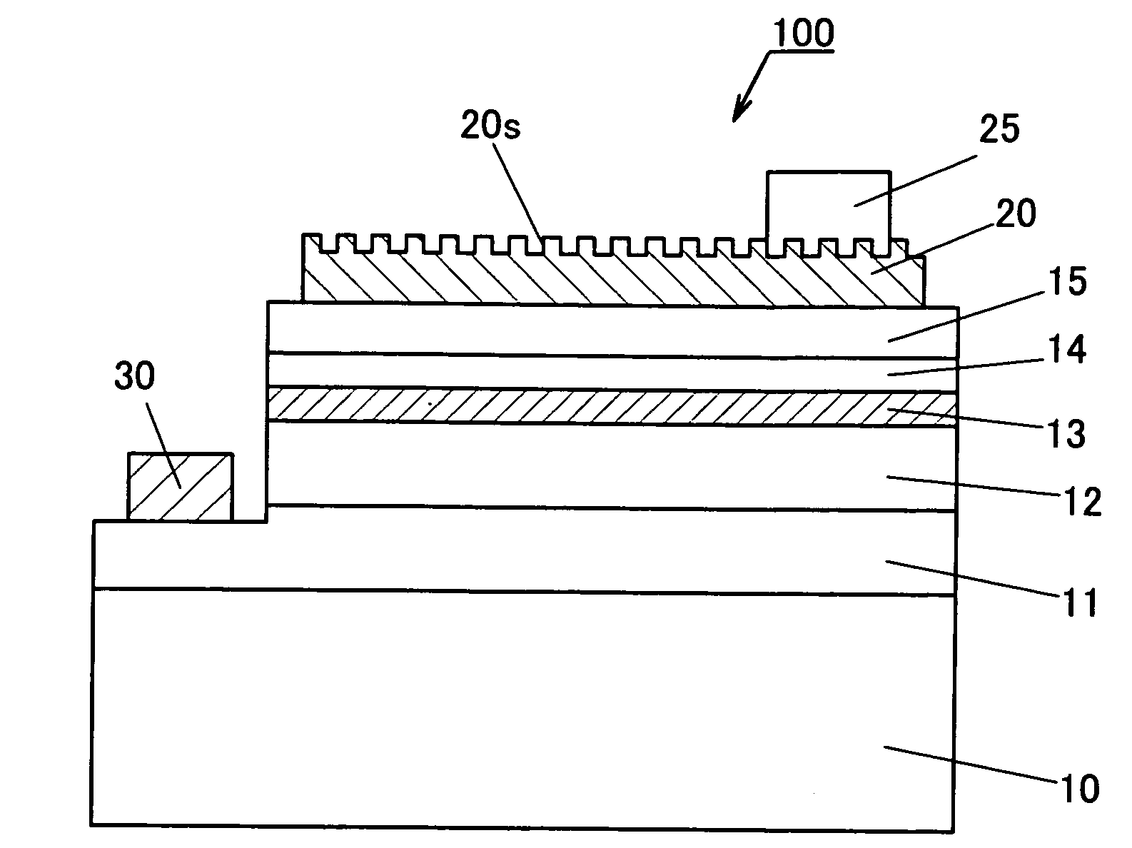
[0037]FIG. 1 is a cross-sectional view of the configuration of a Group III nitride-based compound semiconductor light-emitting device 100 according to Embodiment 1 of the present invention. The Group III nitride-based compound semiconductor light-emitting device 100 includes a sapphire substrate 10; an aluminum nitride (AlN) buffer layer (thickness: about 15 nm) (not illustrated) provided on the substrate 10; and a silicon (Si)-doped GaN n-contact layer 11 (thickness: about 4 μm) formed on the buffer layer. On the n-contact layer 11 is provided an n-cladding layer 12 (thickness: about 74 nm) formed of 10 layer units, each including an undoped In0.1Ga0.9N layer, an undoped GaN layer, and a silicon (Si)-doped GaN layer.

[0038]On the n-cladding layer 12 is provided a light-emitting layer 13 having a multiple quantum well (MQW) structure including alternately stacked eight well layers and eight barrier layers, in which each well layer is formed of an In0.2Ga0.8N layer (thickness: about 3...

embodiment 2

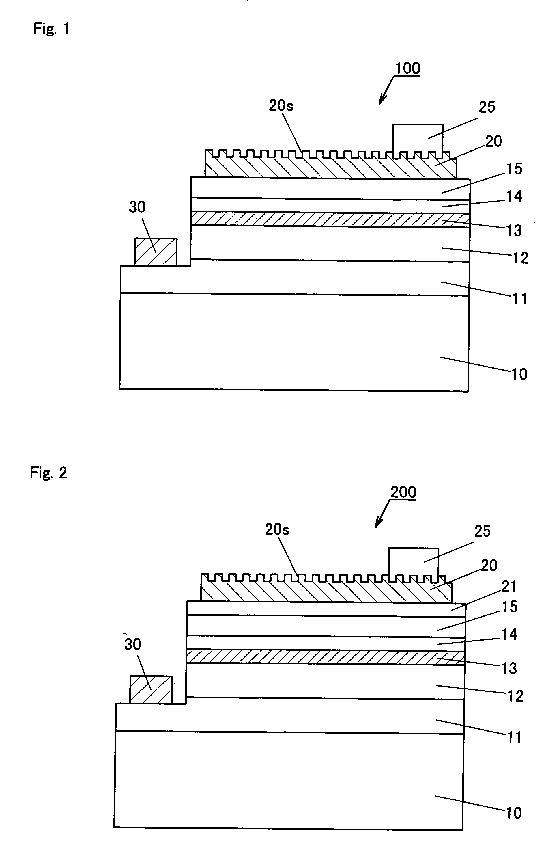
[0058]FIG. 2 is a cross-sectional view of the configuration of a Group III nitride-based compound semiconductor light-emitting device 200 according to Embodiment 2 of the present invention. The Group III nitride-based compound semiconductor light-emitting device 200 shown in FIG. 2 has the same configuration as the Group III nitride-based compound semiconductor light-emitting device 100 shown in FIG. 1, except that a transparent, electrically conductive layer 21 made of indium tin oxide (ITO) and having a thickness of 50 nm (i.e., less than 1 / (4n) of the emission wavelength (470 nm) in the air of the light emitted from the light-emitting layer 13 (wherein n represents the refractive index of ITO)) is provided between the p-type GaN layer 15 and the transparent electrode 20 made of niobium titanium oxide (niobium: 3 mol %). The transparent, electrically conductive layer 21 made of ITO having low resistivity is envisaged to exhibit the effect of reducing the diffusion resistance (in a...

embodiment 3

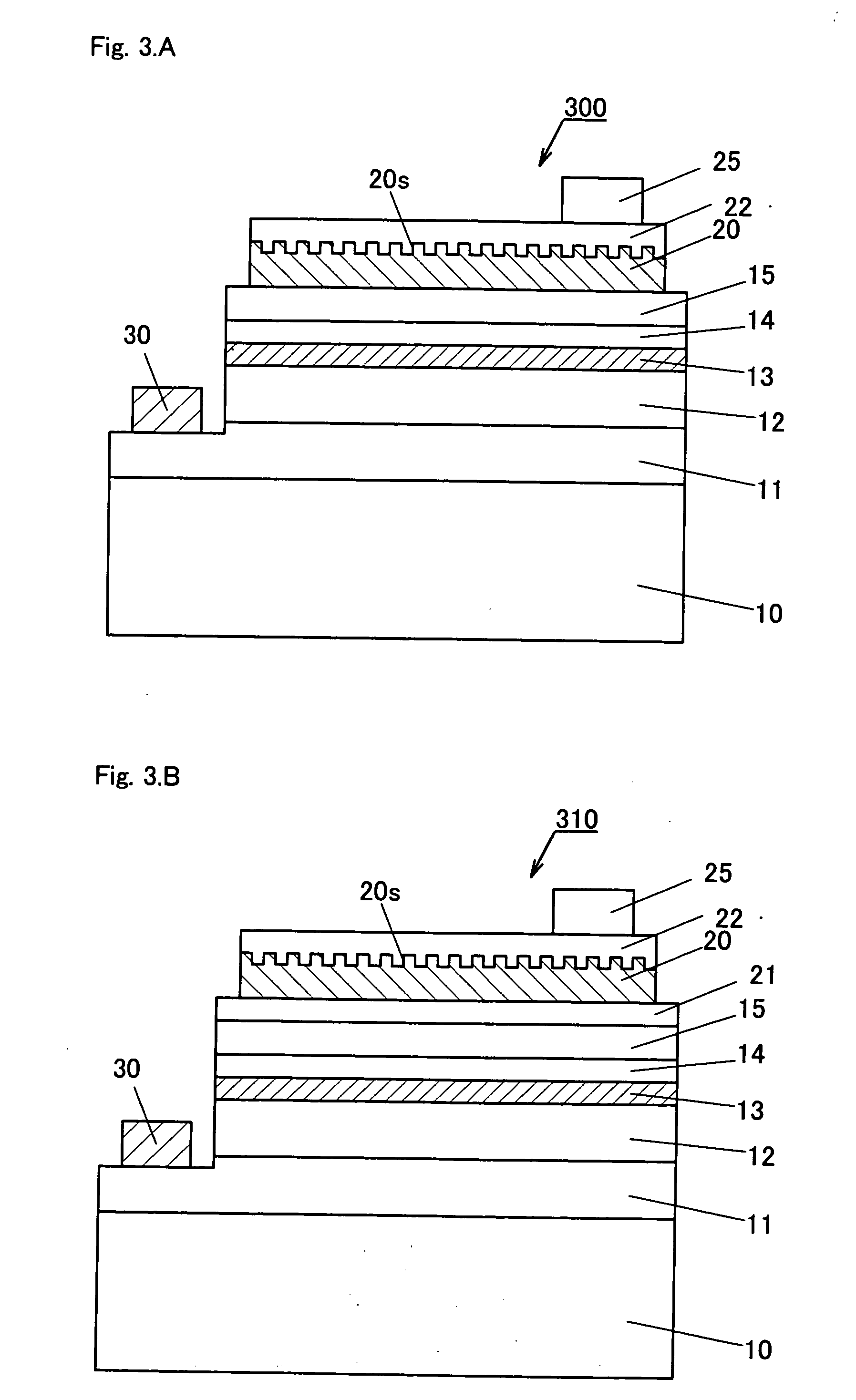
[0059]FIG. 3A is a cross-sectional view of the configuration of a Group III nitride-based compound semiconductor light-emitting device 300 according to Embodiment 3 of the present invention. The Group III nitride-based compound semiconductor light-emitting device 300 shown in FIG. 3A has the same configuration as the Group III nitride-based compound semiconductor light-emitting device 100 shown in FIG. 1, except that the top surface of the transparent electrode 20 made of niobium titanium oxide (niobium: 3 mol %) is covered with a transparent, electrically conductive layer 22 made of indium tin oxide (ITO) and having a thickness of 200 nm. By virtue of addition of the transparent, electrically conductive layer 22 made of ITO, the diffusion resistance (in a plane direction) of the positive electrode can be reduced. FIG. 3B is a cross-sectional view of the configuration of a Group III nitride-based compound semiconductor light-emitting device 310, which is a modification of Embodiment...


PUM

PropertyMeasurementUnit
refractive indexaaaaaaaaaa
total thicknessaaaaaaaaaa

Abstract

The refractive index of a titanium oxide layer is modified by adding an impurity (e.g., niobium (Nb)) thereto within a range where good electrical conductivity is obtained. The Group III nitride-based compound semiconductor light-emitting device of the invention includes a sapphire substrate, an aluminum nitride (AlN) buffer layer, an n-contact layer, an n-cladding layer, a multiple quantum well layer (emission wavelength: 470 nm), a p-cladding layer, and a p-contact layer. On the p-contact layer is provided a transparent electrode made of niobium titanium oxide and having an embossment. An electrode is provided on the n-contact layer. An electrode pad is provided on a portion of the transparent electrode. Since the transparent electrode is formed from titanium oxide containing 3% niobium, the refractive index with respect to light (wavelength: 470 nm) becomes almost equal to that of the p-contact layer. Thus, the total reflection at the interface between the p-contact layer and the transparent electrode can be avoided to the smallest possible extent. In addition, by virtue of the embossment, light extraction performance is increased by 30%.

Description

BACKGROUND OF THE INVENTION[0001]1. Field of the Invention[0002]The present invention relates to a Group III nitride-based compound semiconductor light-emitting device exhibiting improved light extraction performance. As used herein, “Group III nitride-based compound semiconductor” encompasses a semiconductor represented by the formula AlxGayIn1-x-yN (0≦x≦1, 0≦y≦1, 0≦x+y≦1); such a semiconductor containing a predetermined element so as to attain, for example, an n-type / p-type conduction; and such a semiconductor in which a portion of a Group III element is substituted by B or Tl, and a portion of the Group V element is substituted by P, As, Sb, or Bi.[0003]2. Background Art[0004]Generally, Group III nitride-based compound semiconductor light-emitting devices employ a Group III nitride-based compound semiconductor having a refractive index as high as about 2.5. Therefore, in such devices, total reflection of light is likely to occur at the interface between a layer made of a Group II...

Claims


Application Information

Patent Timeline
Patent Type & Authority Applications(United States)
IPC IPC(8): H01L33/00H01L33/42H01L33/06H01L33/22H01L33/32H01L33/38
CPCH01L33/32H01L33/42H01L2933/0091
Inventor MORIYAMA, MIKIGOSHONOO, KOICHIHITOSUGI, TAROHASEGAWA, TETSUYA
Owner TOYODA GOSEI CO LTD
Why Eureka
Eureka Blog
Learn More