Eureka AIR delivers breakthrough ideas for toughest innovation challenges, trusted by R&D personnel around the world.

Method for producing a group III nitride semiconductor light-emitting device

a technology of nitride and light-emitting devices, which is applied in the direction of semiconductor devices, basic electric elements, electrical appliances, etc., can solve the problems of crystal damage, increase production cost, and increase production cost, so as to improve light extraction performance and reduce production cost. , the effect of easy formation of concave and convex configuration

Active Publication Date: 2015-02-03
TOYODA GOSEI CO LTD
View PDF21 Cites 0 Cited by
  • Summary
  • Abstract
  • Description
  • Claims
  • Application Information

AI Technical Summary

Benefits of technology

[0012]In view of the foregoing, an object of the present invention is to easily form a concave and convex configuration on a light output surface of a Group III nitride semiconductor light-emitting device.
[0016]Preferably, the p cladding layer has an Mg concentration of 1.2×10²⁰ / cm3 or more. This is because when the convex density is high and the depth of concave and the height of convex are large, light extraction performance can be further improved. Moreover, the p cladding layer preferably has an Mg concentration of 1×10²¹ / cm3 or less. When the Mg concentration is higher, the crystallinity of the p cladding layer is deteriorated. More preferably, the p cladding layer has an Mg concentration of 1.2×10²⁰ / cm3 to 5×10²⁰ / cm3. The Mg concentration is determined by obtaining in advance a proportional relationship between the Mg doping amount and the supply amount of Mg raw material gas when the p cladding layer is formed in a flat film instead of a concave and convex configuration and calculating based on the supply amount of Mg raw material gas by the measured proportional relationship.
[0017]Preferably, the p cladding layer is grown at a pressure of 1 kPa to 100 kPa. When the pressure falls within this range, a concave and convex configuration can be formed such that the convex density is high and the depth of concave and the height of convex are large, resulting in improvement of light extraction performance. More preferably, the pressure is 5 kPa to 70 kPa.
[0022]The present invention can easily form a concave and convex configuration to improve light extraction performance. Therefore, the production cost can be reduced.

Problems solved by technology

Therefore, the production is complicated due to multiple processes, resulting in an increase of the production cost.
A method for providing a concave and convex configuration through processing requires a specific process after crystal growth, resulting in an increase of the production cost.
In addition, some crystal damage remains and a special etching is required because the Group III nitride semiconductor has high hardness.
However, a p-type Group III nitride semiconductor is difficult to be grown thick while maintaining a good crystallinity.
This may reduce the steepness of the interface and degrade the light emission performance.
When the off-angle of the substrate is increased, there is a problem that crystallinity is considerably reduced.

Method used


Image

  • Method for producing a group III nitride semiconductor light-emitting device
  • Method for producing a group III nitride semiconductor light-emitting device
  • Method for producing a group III nitride semiconductor light-emitting device

Examples


embodiment 1

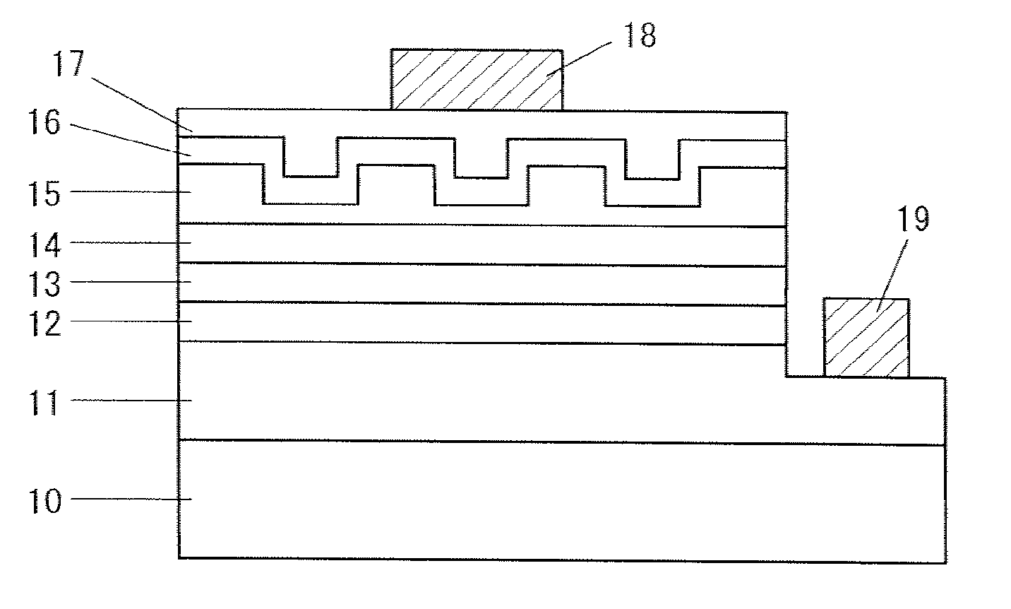
[0029]FIG. 1 shows the configuration of a Group III nitride semiconductor light-emitting device according to Embodiment 1. The Group III nitride semiconductor light-emitting device according to Embodiment 1 has a sapphire substrate 10. On the sapphire substrate 10, via an AlN buffer layer (not illustrated), sequentially formed are an n-type contact layer 11 of n-GaN having a thickness of 4 μm, an ESD layer 12 of i-GaN having a thickness of 300 nm and n-GaN having a thickness of 30 nm, an n cladding layer 13 being a multilayer having a thickness of about 64 nm, in which fifteen layer units, each unit being formed of i-InGaN, i-GaN and n-GaN, are deposited, and a light-emitting layer 14 having a MQW structure where an InGaN well layer having a thickness of 3 nm and a GaN barrier layer having a thickness of 4 nm are alternately deposited eight times. On the light-emitting layer 14, sequentially formed are a p cladding layer 15 of p-AlGaN having a thickness of 12 nm and a p contact laye...


PUM


Abstract

The present invention provides a Group III nitride semiconductor light-emitting device exhibiting improved light extraction performance. In the production method, a p cladding layer of p-AlGaN is formed by the MOCVD method on a light-emitting layer at a pressure of 30 kPa and with an Mg concentration of 1.5×10²⁰ / cm3. A plurality of regions with a nitrogen polarity is formed in the crystals with a Group III element polarity, and thus the p cladding layer has a hexagonal columnar concave and convex configuration on the surface thereof. Subsequently, a p contact layer of GaN is formed by the MOCVD method, in a film along the concave and convex configuration on the p cladding layer.

Description

BACKGROUND OF THE INVENTION[0001]1. Field of the Invention[0002]The present invention relates to a method for producing a Group III nitride semiconductor light-emitting device exhibiting improved light extraction performance.[0003]2. Background Art[0004]A method for providing a concave and convex configuration on a light output surface has been proposed to improve the light extraction performance of the Group III nitride semiconductor light-emitting device.[0005]In a known method for providing a concave and convex configuration, a reversed polarity layer is used. A Group III nitride semiconductor is usually grown in a +c axis direction and thus has a Group III element polarity. However, a reversed polarity layer includes at least a portion thereof with a nitrogen polarity opposite to a Group III element polarity. The reversed polarity layer can be formed by doping a high concentration of Mg into the crystal. (For example, refer to Japanese Patent Application Laid-Open (kokai) No. 20...

Claims


Application Information

Patent Timeline
Patent Type & Authority Patents(United States)
IPC IPC(8): H01L21/00H01L33/00H01L33/14
CPCH01L33/007H01L33/14
Inventor NAKADA, NAOYUKIUSHIDA, YASUHISA
Owner TOYODA GOSEI CO LTD
Why Eureka
Eureka Blog
Learn More