Organic light emitting display device

Active Publication Date: 2015-03-26
LG DISPLAY CO LTD
View PDF6 Cites 47 Cited by
  • Summary
  • Abstract
  • Description
  • Claims
  • Application Information

AI Technical Summary

Benefits of technology

[0015]An aspect of the present invention is directed to provide an organic light

Problems solved by technology

However, in the general organic light emitting display device, due to a non-uniformity of a manufacturing process of a thin film transistor (TFT)

Method used


Image

  • Organic light emitting display device
  • Organic light emitting display device
  • Organic light emitting display device

Examples


first embodiment

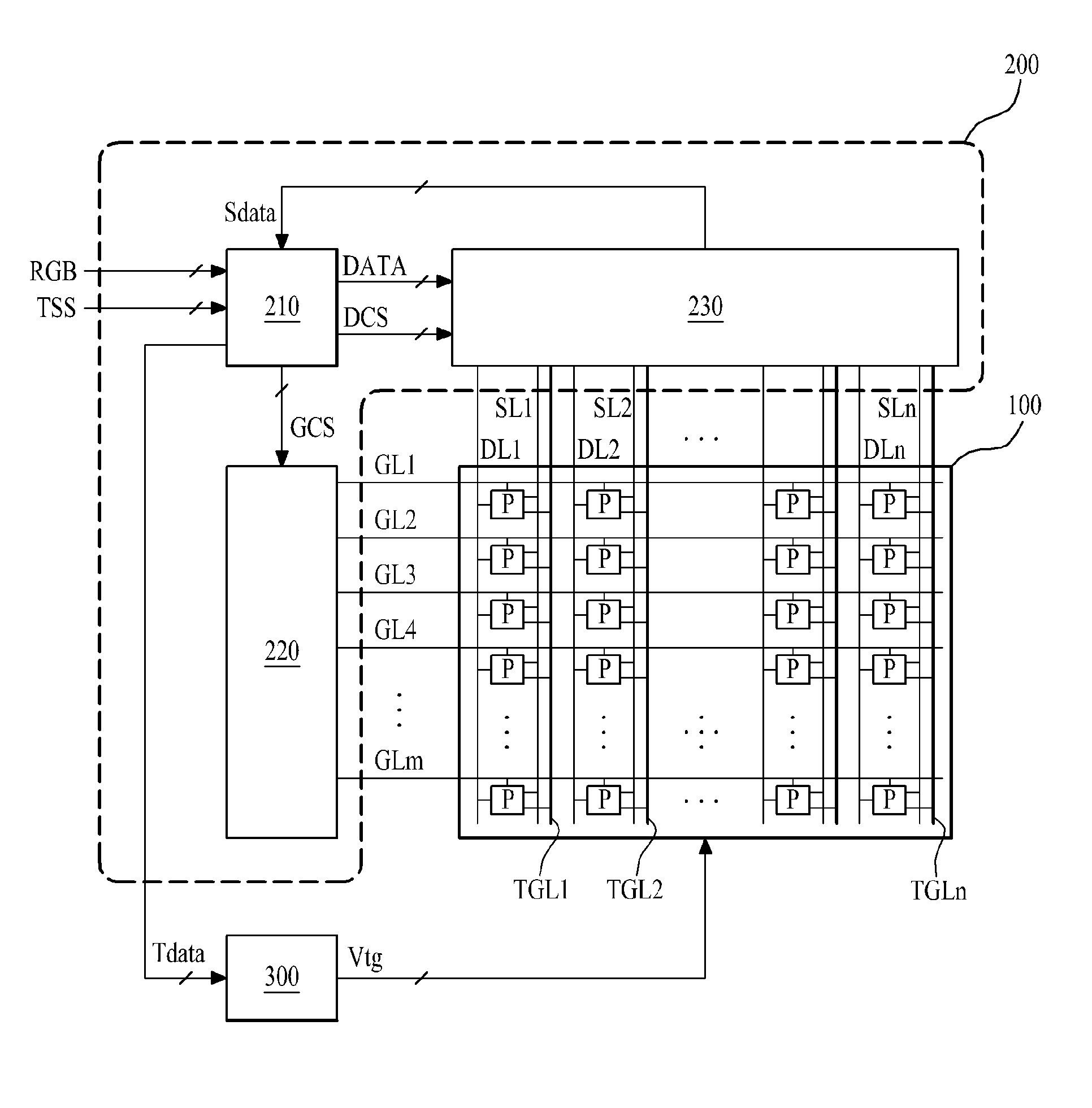
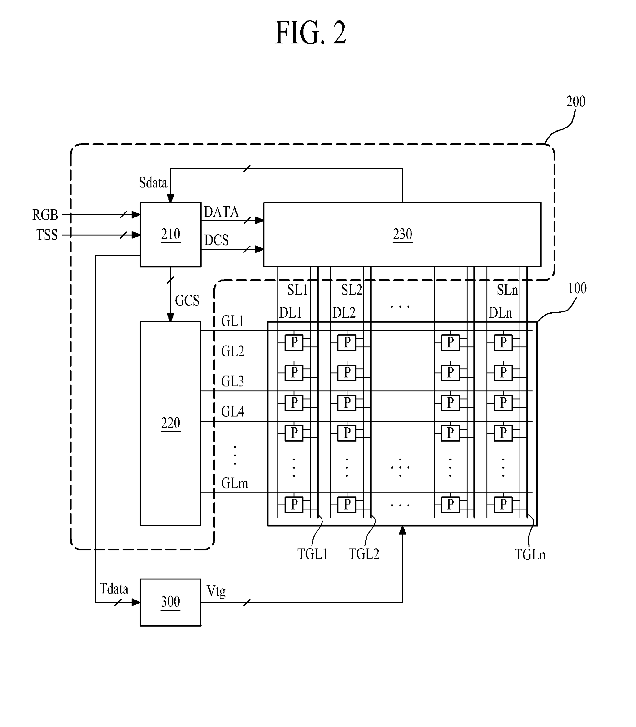
[0043]FIG. 2 is a diagram for describing an organic light emitting display device according to the present invention. FIG. 3 is a diagram for describing a structure of an ith pixel of FIG. 2. FIG. 4 is a cross-sectional view for describing a structure of a driving transistor of FIG. 3.

[0044]Referring to FIGS. 2 to 4, the organic light emitting display device according to the first embodiment of the present invention includes a display panel 100, a panel driver 200, and a voltage supply unit 300.

[0045]The display panel 100 includes a plurality of data lines DL1 to DLn, a plurality of gate lines GL1 to GLm, a plurality of upper gate voltage lines TGL1 to TGLn (or a plurality of second gate voltage lines), a plurality of sensing lines SL1 to SLn, and a plurality of pixels P.

[0046]The plurality of data lines DL1 to DLn are arranged at certain intervals in the display panel 100. When the display panel 100 operates in a display mode, each of the plurality of data lines DL1 to DLn may be u...

second embodiment

[0093]FIG. 11 is a diagram for describing a pixel structure in an organic light emitting display device according to the present invention. The pixel structure is implemented by changing a structure of each of the first and second switching transistors T1 and T2. Hereinafter, only elements which differ from the above-described elements will be described.

[0094]First, a driving transistor Tdr included in each of a plurality of pixels P includes a gate electrode, a source electrode, and a drain electrode.

[0095]A first switching transistor T1, similar to the driving transistor Tdr of FIG. 4, includes a lower gate electrode 111 and an upper gate electrode 117 (T1—tg) which overlap each other with a semiconductor layer 113 therebetween. Here, the lower gate electrode 111 is connected to a first gate signal line GLa adjacent thereto, and the upper gate electrode 117 (T1—tg) is connected to an upper gate voltage line TGLi adjacent thereto. Similar to the driving transistor Tdr, a threshold ...

third embodiment

[0103]The organic light emitting display device according to the present invention applies, in common or separately, the upper gate voltage Vtg to respective upper gate electrodes Tdr_tg, T1—tg and T2—tg of the driving transistor Tdr and first and second switching transistors T1 and T2 of each pixel P to restore a threshold voltage shift of each of the transistors T1, T2 and Tdr of each pixel P to the normal compensation range, thereby enhancing a reliability of the transistors T1, T2 and Tdr included in each pixel P and the display panel 100.

[0104]FIG. 13 is a diagram for describing a modification example of a plurality of upper gate voltage lines in the organic light emitting display device according to the first to third embodiments of the present invention. Hereinafter, only elements which differ from the above-described elements will be described.

[0105]The plurality of upper gate voltage lines TGL1 to TGLn are formed in parallel with the plurality of data lines DL1 to DLn, and ...


PUM


Abstract

Disclosed is an organic light emitting display device. The organic light emitting display includes a display panel including a plurality of pixels, which are respectively formed in a plurality of pixel areas defined by crossings of a plurality of gate lines and a plurality of data lines, a plurality of sensing lines, and a plurality of second gate voltage lines connected to the plurality of pixels, a panel driver to drive the display panel in a display mode or a sensing mode, to sense a threshold voltage of at least one transistor to generate a sensing data in the sensing mode, and generate a second gate voltage data in the display mode, and a voltage supply unit to generate a second gate electrode voltage corresponding to the second gate voltage data, and apply a second gate electrode voltage to a second gate electrode of the transistor.

Description

CROSS-REFERENCE TO RELATED APPLICATION[0001]This application claims the benefit of the Korean Patent Application No. 10-2013-0114163 filed on Sep. 25, 2013, which is hereby incorporated by reference for all purposes as if fully set forth herein.BACKGROUND[0002]1. Field of the Disclosure[0003]Embodiments of the present invention relate to a flat panel display (FPD) device. More particularly, the embodiments relate to an organic light emitting display device including a thin film transistor (TFT).[0004]2. Discussion of the Related Art[0005]Because of advantages such as a thin profile, lighting thereof and low power consumption, flat panel display devices are widely used. In the flat panel display devices, a liquid crystal display (LCD) device and an organic light emitting display device including a thin film transistor (TFT) are good in resolution, color display, and image quality, and thus are commercialized as display devices for notebook computers, tablet computers, and desktop com...

Claims


Application Information

Patent Timeline
IPC IPC(8): G09G3/32
CPCG09G3/3258G09G3/3291G09G2310/08G09G2310/0272G09G2300/0809G09G3/3233G09G2310/0218G09G2320/0295G09G2320/043G09G3/32
Inventor SHIM, JONG SIKLEE, SI KYU
Owner LG DISPLAY CO LTD
Why Eureka
Try Eureka