Low temperature poly-silicon thin film transistor, fabricating method thereof, array substrate and display device

a thin film technology, applied in the field of display technology, can solve the problems of reducing the reliability and yield of thin film transistors, poor contact between sources, etc., and achieve the effect of improving the reliability and yield of low temperature polysilicon thin film transistors, reducing contact resistance, and reducing the power consumption of driving circuits

Inactive Publication Date: 2016-11-10
BOE TECH GRP CO LTD +1
View PDF8 Cites 7 Cited by
  • Summary
  • Abstract
  • Description
  • Claims
  • Application Information

AI Technical Summary

Benefits of technology

[0025]In the embodiments of the present invention, since the thicknesses of the source contact region and the drain contact region are greater than that of the channel region, even if certain recesses are formed in the source contact region and the drain contact region due to over etching during etching the via hole, the source and the drain still have relatively large contact areas with the active layer, as a result, reliability and yield of the low temperature poly-silicon thin film transistor are improved, meanwhile, contact resistance is decreased and both turn-on voltage and power consumption of a driving circuit are lowered. Moreover, in the channel region which is relatively thin, poly-silicon grains are prone to growing laterally, so that the grains have relatively large lateral size, and the active layer of the thin film transistor is anisotropic, and thus the active layer of the thin film transistor has good conductivity when the thin film transistor is turned on.

Problems solved by technology

However, as shown in FIG. 2, in the prior art, an over etching phenomenon is likely to occur during etching the via hole, resulting in poor contact between the source 12, the drain 13 and the active layer 11 after the source 12 and the drain 13 are formed, thus reducing the reliability and yield of the thin film transistor.

Method used


Image

  • Low temperature poly-silicon thin film transistor, fabricating method thereof, array substrate and display device
  • Low temperature poly-silicon thin film transistor, fabricating method thereof, array substrate and display device
  • Low temperature poly-silicon thin film transistor, fabricating method thereof, array substrate and display device

Examples


Embodiment Construction

[0034]Specific implementations of the present invention will be described in detail below with reference to the accompanying drawings. It should be understood that the specific implementations described here are only used for illustrating and explaining the present invention but not for limiting the present invention.

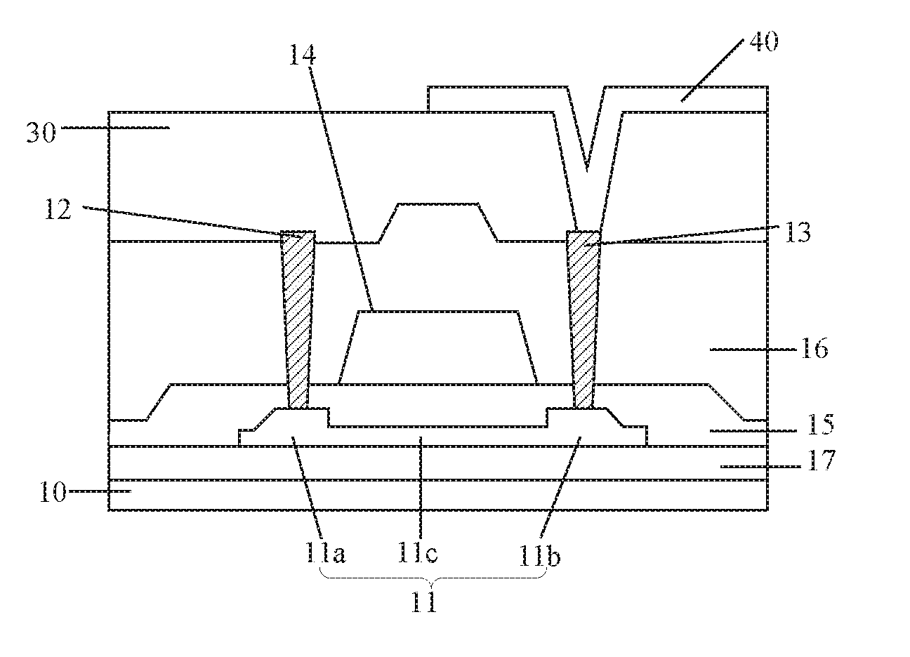
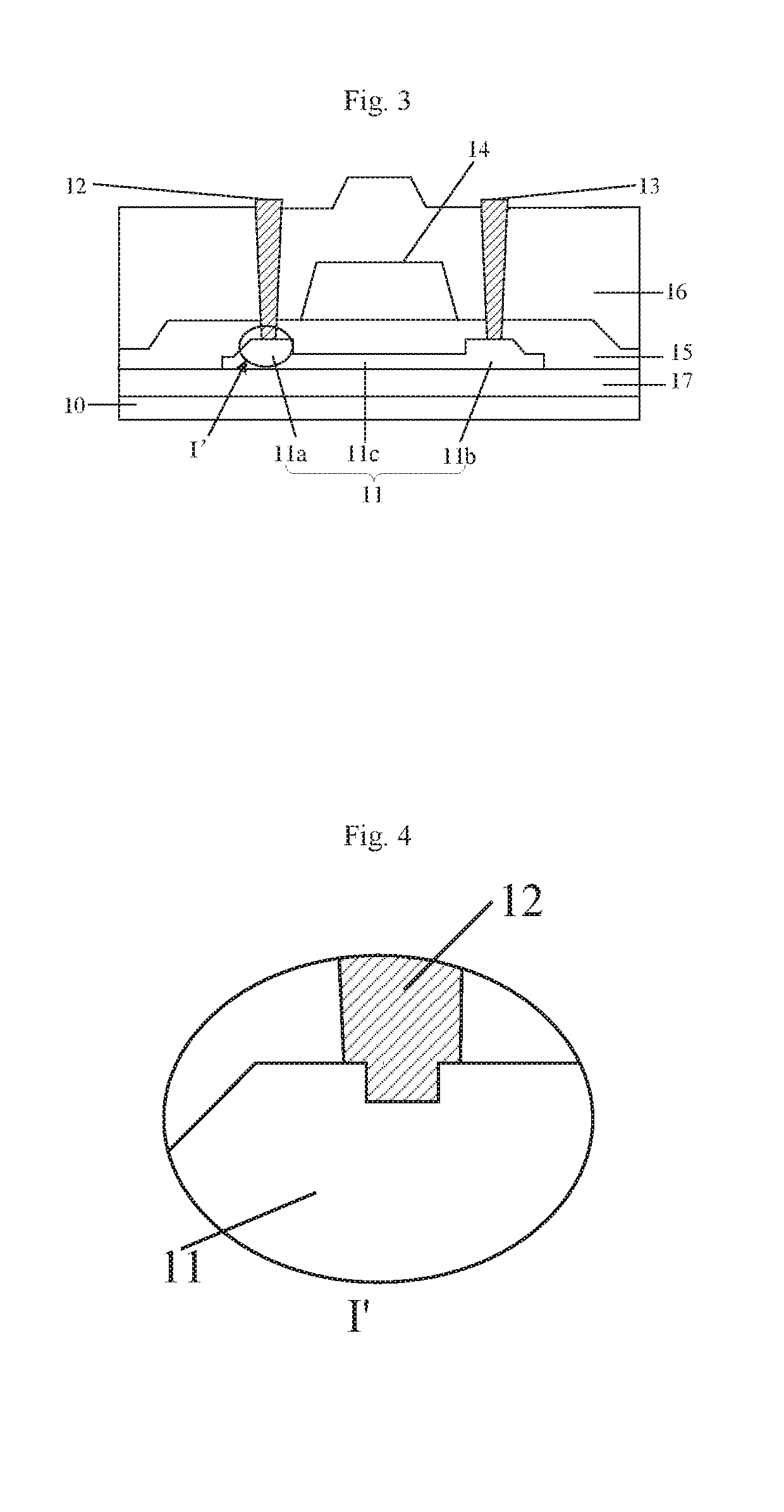
[0035]As a first aspect of the present invention, the embodiments of the present invention provide a low temperature poly-silicon thin film transistor. As shown in FIG. 3, the low temperature poly-silicon thin film transistor comprises an active layer 11, a source 12 and a drain 13. The active layer 11 comprises a source contact region 11a, a drain contact region 11b, and a channel region 11c located between the source contact region 11a and the drain contact region 11b. The source 12 is provided above the source contact region 11a and connected to the source contact region 11a through a source via hole, and the drain 13 is provided above the drain contact region 11b an...


PUM

PropertyMeasurementUnit
thicknessesaaaaaaaaaa
temperatureaaaaaaaaaa
thicknessaaaaaaaaaa

Abstract

Embodiments of the present invention disclose a low temperature poly-silicon thin film transistor and a method of fabricating the same, an array substrate, and a display device. The low temperature poly-silicon thin film transistor comprises an active layer, a source and a drain, wherein the active layer comprises a source contact region, a drain contact region, and a channel region located between the source contact region and the drain contact region, the source is provided above and connected to the source contact region, the drain being provided above and connected to the drain contact region, and thicknesses of the source contact region and the drain contact region are both larger than that of the channel region.

Description

FIELD OF THE INVENTION[0001]The present invention relates to the field of display technology, and particularly relates to a low temperature poly-silicon thin film transistor, a method of fabricating a low temperature poly-silicon thin film transistor, an array substrate comprising the low temperature poly-silicon thin film transistor, and a display device comprising the array substrate.BACKGROUND OF THE INVENTION[0002]A low temperature poly-silicon (LTPS) thin film transistor liquid crystal display, compared with the traditional amorphous silicon thin film transistor liquid crystal displays, has high electron mobility, which can not only effectively reduce the area of a thin film transistor device to improve aperture ratio, but also reduce power consumption while enhancing brightness of the display. In addition, the relatively high electron mobility allows part of drive circuits to be integrated onto a glass substrate to reduce cost of the drive circuits, and can further greatly enh...

Claims


Application Information

Patent Timeline
Patent Type & Authority Applications(United States)
IPC IPC(8): H01L27/12H01L29/417H01L29/423H01L21/265H01L21/768H01L29/66H01L21/306H01L21/308H01L29/786H01L23/535
CPCH01L27/1285H01L27/1222H01L29/78675H01L29/78618H01L29/41733H01L21/265H01L23/535H01L21/76895H01L29/66757H01L21/30604H01L21/3085H01L29/42384G02F1/1362H01L27/1214H01L29/06H01L29/0847H01L29/6675H01L29/786H01L29/78672H01L29/41783
Inventor LI, XINGHUABAO, JUNPING
Owner BOE TECH GRP CO LTD
Why Eureka
Try Eureka