Thin film transistor array substrate and display device

a thin film transistor and array substrate technology, applied in the field of display, can solve the problems of unsatisfactory lack of novel design, etc., and achieve the effect of display quality, improving wiring efficiency, and improving the reliability of the thin film transistor

Active Publication Date: 2018-12-25
BOE TECH GRP CO LTD
View PDF6 Cites 0 Cited by
  • Summary
  • Abstract
  • Description
  • Claims
  • Application Information

AI Technical Summary

Benefits of technology

[0006]The present disclosure provides a novel thin film transistor array substrate, in which wiring efficiency is improved, and reliability of the thin film transistor and display quality may be improved.

Problems solved by technology

Currently, the thin film transistor array substrate normally has a single kind of structure and thus lack novel design.
Further, wiring efficiency of the existing thin film transistor array substrate is still needed to be improved and reliability of the thin film transistor and display quality both are still not perfect.

Method used


Image

  • Thin film transistor array substrate and display device
  • Thin film transistor array substrate and display device
  • Thin film transistor array substrate and display device

Examples


Embodiment Construction

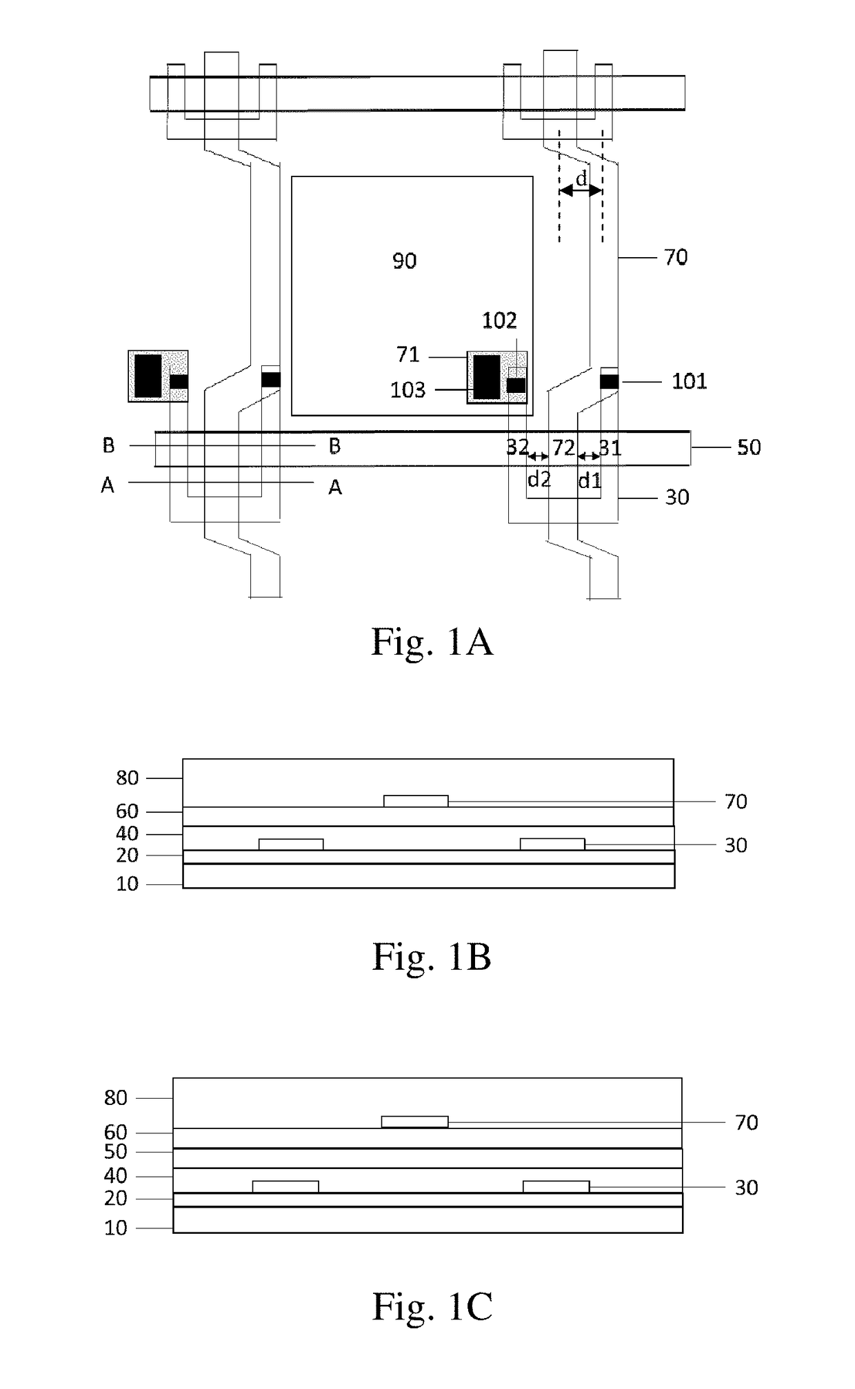
[0041]The present disclosure provides a new thin film transistor array substrate and a display device. The thin film transistor array substrate includes: a substrate, and a first signal line and a thin film transistor formed on the substrate. An active layer of the thin film transistor and the first signal line are located on different layers over the substrate and projections of them on a plane where the substrate is located overlap at at least two positions. The portion of the active layer overlapping with the projection of the first signal line on the plane where the substrate is located is termed as an active layer overlapping section.

[0042]In an embodiment, in a thin film transistor array substrate, the active layer overlapping section includes a folding section, or includes a pattern with at least a side opening. These two structures both may achieve overlapping at at least two positions between the projections of the active layer of the thin film transistor and the first sign...


PUM


Abstract

The present disclosure provides a thin film transistor array substrate and a display device implementing the same. The thin film transistor array substrate includes a substrate; a first signal line formed on the substrate; and a thin film transistor formed on the substrate, and an active layer of the thin film transistor and the first signal line are located on different layers above the substrate and projections of them on a plane where the substrate is located overlap with each other at at least two positions. The present disclosure may improve wiring efficiency and reliability of the thin film transistor array substrate.

Description

CROSS-REFERENCE TO RELATED APPLICATIONS[0001]The present application claims priority to Chinese Patent Application NO. 201620442368.8, filed on May 16, 2016, entitled “THIN FILM TRANSISTOR ARRAY SUBSTRATE AND DISPLAY DEVICE”, which is incorporated herein by reference in its entirety.BACKGROUND OF THE INVENTIONField of the Invention[0002]The present disclosure relates to technical field of display, and particularly to a thin film transistor array substrate and a display device.Description of the Related Art[0003]Active matrix display device is a display device in which thin film transistor is configured for drive of pixels for display, and possesses advantages of thin thickness, light weight, low power consumption, low radiation and low cost, and thus becomes mainstream display technology.[0004]The active matrix display device commonly includes a thin film transistor (TFT) array substrate. The thin film transistor array substrate includes a plurality of gate lines in a first directio...

Claims


Application Information

Patent Timeline
Patent Type & Authority Patents(United States)
IPC IPC(8): H01L27/12H01L29/49H01L29/786
CPCH01L27/124H01L27/12H01L29/78678H01L29/4908H01L29/78675H01L27/127H01L29/78696H01L27/1222
Inventor LONG, CHUNPINGQIAO, YONG
Owner BOE TECH GRP CO LTD
Why Eureka
Try Eureka