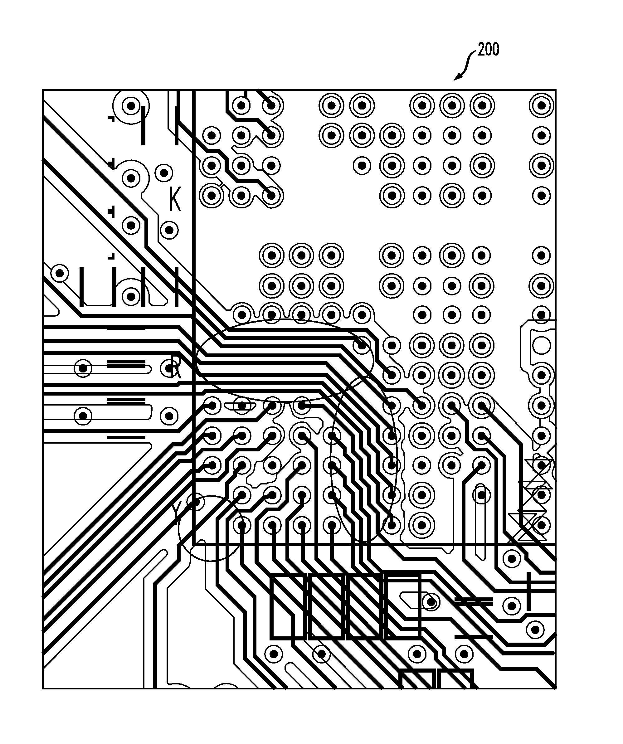
Partially Depopulated Interconnection Arrays for Packaged Semiconductor Devices and Printed Circuit Boards
a technology of interconnection arrays and semiconductor devices, applied in the direction of final product manufacturing, semiconductor/solid-state device details, sustainable manufacturing/processing, etc., can solve problems such as inhibiting ability
- Summary
- Abstract
- Description
- Claims
- Application Information
AI Technical Summary
Benefits of technology
Problems solved by technology
Method used
Image


Examples
Embodiment Construction
[0015]Detailed illustrative embodiments of the present invention are disclosed herein. However, specific structural and functional details disclosed herein are merely representative for purposes of describing example embodiments of the present invention. Embodiments of the present invention may be embodied in many alternative forms and should not be construed as limited to only the embodiments set forth herein. Further, the terminology used herein is for the purpose of describing particular embodiments only and is not intended to be limiting of example embodiments of the invention.
[0016]As used herein, the singular forms “a,”“an,” and “the,” are intended to include the plural forms as well, unless the context clearly indicates otherwise. It further will be understood that the terms “comprises,”“comprising,”“has,”“having,”“includes,” and / or “including” specify the presence of stated features, steps, or components, but do not preclude the presence or addition of one or more other feat...
PUM
 Abstract
Description
Claims
Application Information
 - R&D
- Intellectual Property
- Life Sciences
- Materials
- Tech Scout
- Unparalleled Data Quality
- Higher Quality Content
- 60% Fewer Hallucinations
Browse by: Latest US Patents, China's latest patents, Technical Efficacy Thesaurus, Application Domain, Technology Topic, Popular Technical Reports.
© 2025 PatSnap. All rights reserved.Legal|Privacy policy|Modern Slavery Act Transparency Statement|Sitemap|About US| Contact US: help@patsnap.com