
System-in-package module and method for forming the same

Active Publication Date: 2015-09-24
QUANTA COMPUTER INC
View PDF9 Cites 0 Cited by
  • Summary
  • Abstract
  • Description
  • Claims
  • Application Information

AI Technical Summary

Benefits of technology

The patent describes a method for making a system-in-package module by placing a substrate with multiple packaging regions, each containing a chip and a dam. A thermal conductive sheet is placed in each cavity where the chip is located, and the substrate is then diced to create separate packages. These packages are then bonded to a printed circuit board, where the chip is in thermal contact with the board through the thermal conductive sheet. This method helps to improve the thermal performance of the module.

Problems solved by technology

Namely, if too much heat accumulates in the SiP module, the packaged chips may lose their original function, and the reliability of the product is thus degraded.

Method used


Image

  • System-in-package module and method for forming the same
  • System-in-package module and method for forming the same
  • System-in-package module and method for forming the same

Examples


Embodiment Construction

[0015]The following description is of the best-contemplated mode of implementing the invention. This description is made for the purpose of illustrating the general principles of the invention and should not be taken in a limiting sense. The scope of the invention is best determined by reference to the appended claims.

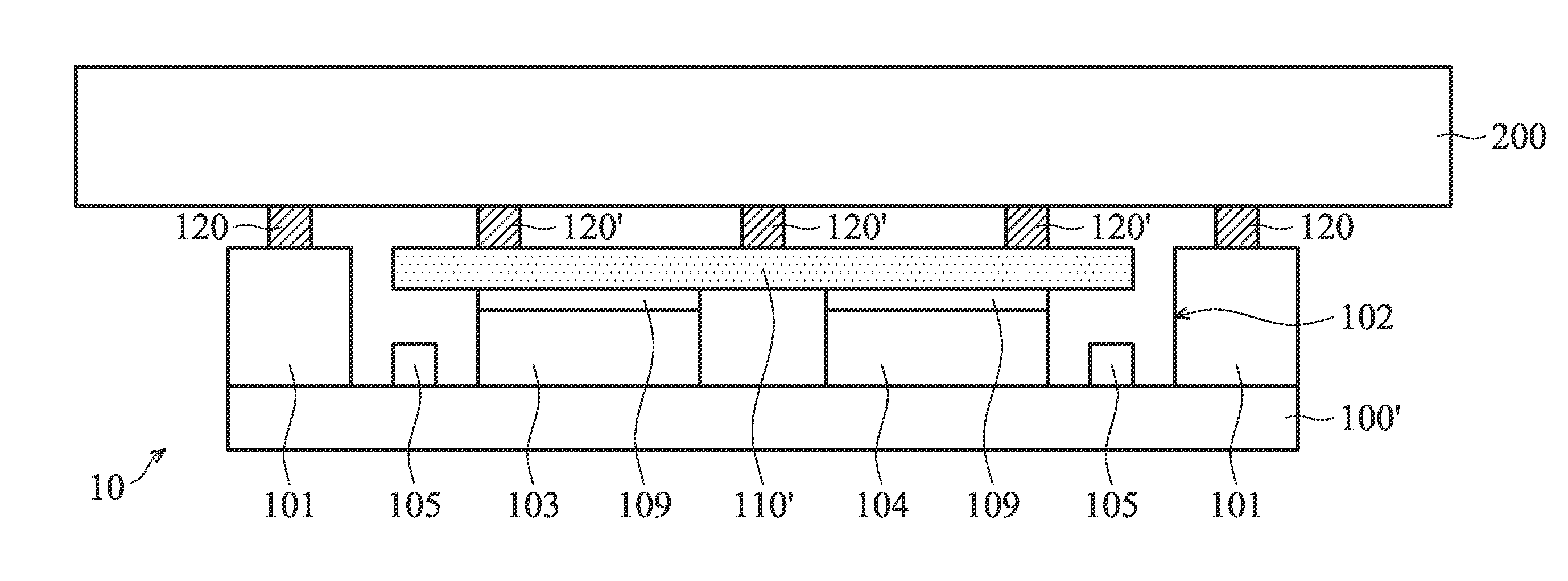
[0016]FIG. 3F is a cross-sectional view of a SiP module according to an embodiment of the disclosure. Refer to FIG. 3. In the embodiment, the SiP module includes a substrate 100′. A dam 101 and chips 103 and 104 are disposed on the substrate 100′. The dam 101 defines a cavity 102 and the chips 103 and 104 are disposed in the cavity 102.

[0017]In the embodiment, the substrate 100′ and the dam 101 may have an interconnect structure (not shown) therein, which may include components such as metal lines, metal vias and pads. The chips 103 and 104 may form an electrical contact by the interconnect structure.

[0018]Passive elements 105 may be optionally disposed on the substrat...


PUM


Abstract

A system-in-package (SiP) module is disclosed. The SiP module includes a substrate and a dam on the substrate. The dam defines a cavity. At least one chip is on the substrate inside the cavity. A printed circuit board (PCB) is bonded to the dam and covers the cavity. A thermal conductive sheet is in the cavity and is disposed between the chip and the PCB. The chip is in thermal contact with the PCB through the thermal conductive sheet. The disclosure also provides a method for manufacturing the SiP module.

Description

CROSS REFERENCE TO RELATED APPLICATIONS[0001]This application claims the priority of Taiwan Patent Application No. 103108594 filed on Mar. 19, 2014, and the entirety of which is incorporated by reference herein.BACKGROUND OF THE INVENTION[0002]1. Field of the Invention[0003]The present invention relates to a package technique, and more particularly to a system-in-package (SiP) module and a method for forming the same.[0004]2. Description of the Related Art[0005]System-in-package (SiP) technique, which may exhibit various configurations such as multi-chip module (MCM), multi-chip package (MCP), chip stack or active / passive elements embedded in the substrate, means that a plurality of integrated circuit (IC) chips and / or passive elements are integrated into a package. Since the SiP technique allows the possibility of hetero-integration, it is extensively applied to various miniature devices. Further, since each of the chips in the SiP module can be developed individually, the SiP tech...

Claims


Application Information

Patent Timeline
IPC IPC(8): H01L23/495H01L25/065H01L25/00H01L21/50
CPCH01L23/49568H01L23/49541H01L25/50H01L21/50H01L25/0655H01L23/4952H01L2224/40137H01L2924/37001H01L23/367H01L24/19H01L24/20H01L24/29H01L24/32H01L24/75H01L24/83H01L24/97H01L25/18H01L2224/2919H01L2224/32245H01L2224/73267H01L2224/75745H01L2224/83191H01L2224/97H01L2924/1421H01L2924/15321H01L2924/19041H01L2924/19042H01L2924/19043H01L2924/19105H01L23/433H01L2924/00014H01L2224/19H01L2224/37099
Inventor SHEN, LI-CHENG
Owner QUANTA COMPUTER INC
Features
  • Generate Ideas
  • Intellectual Property
  • Life Sciences
  • Materials
  • Tech Scout
  • Unparalleled Data Quality
  • Higher Quality Content
  • 60% Fewer Hallucinations
Learn More