Liquid crystal display device
- Summary
- Abstract
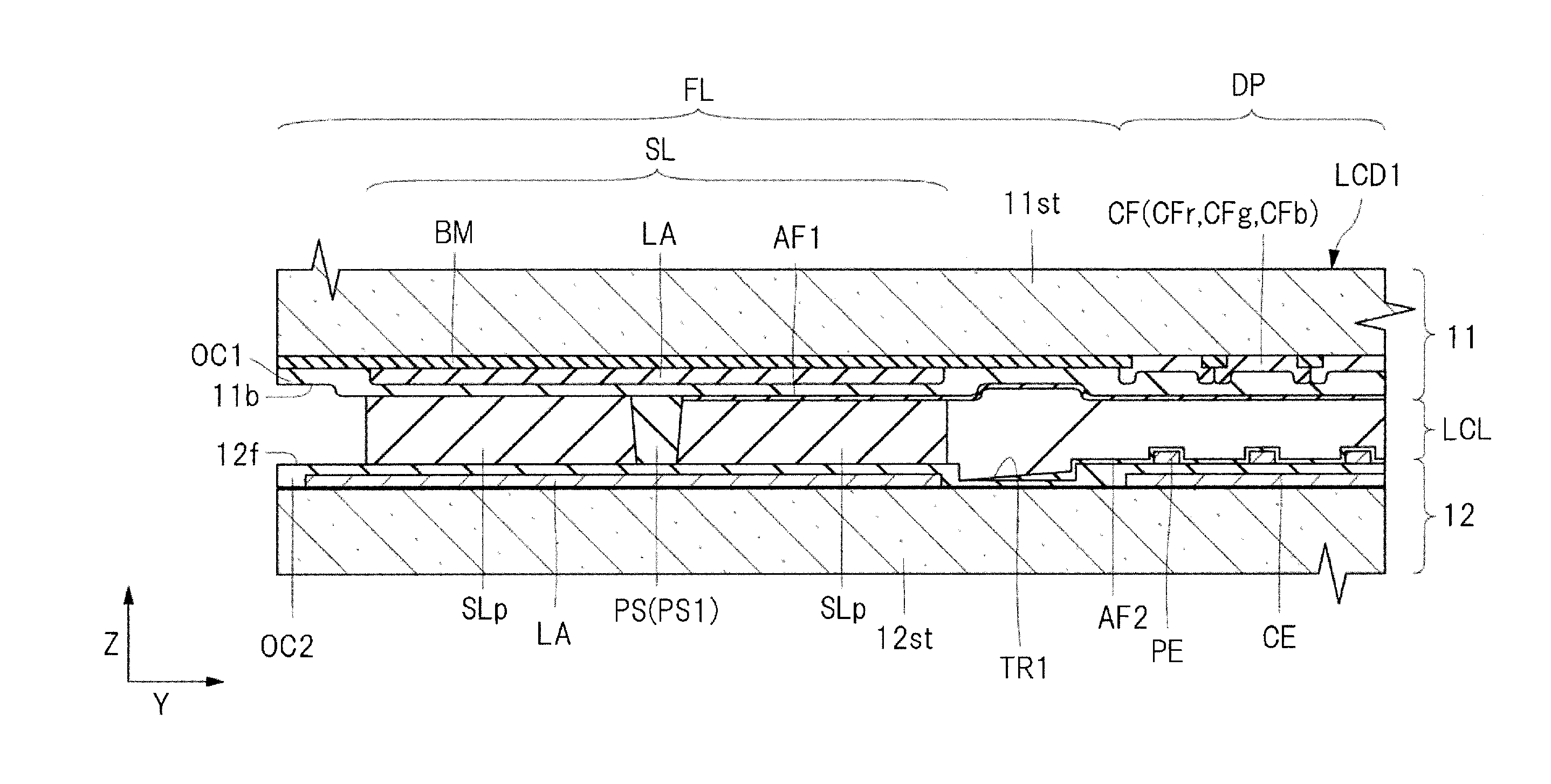
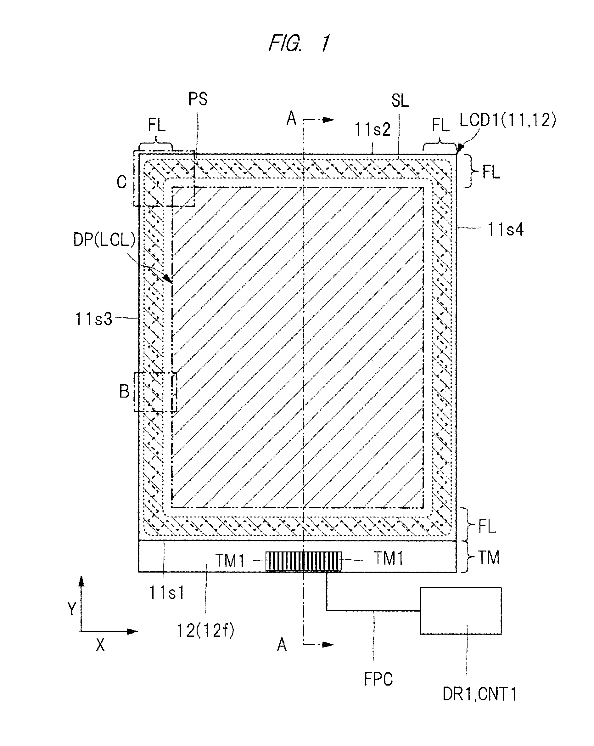
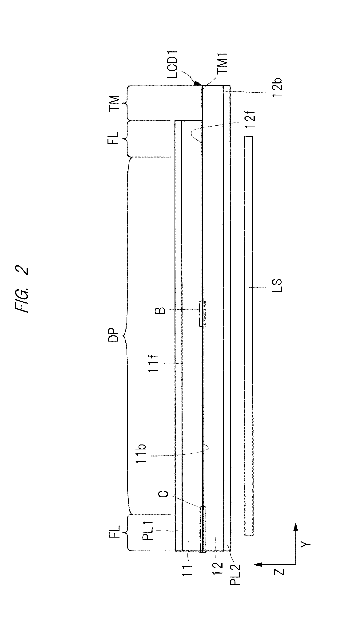
- Description
- Claims
- Application Information
AI Technical Summary
Benefits of technology
Problems solved by technology
Method used
Image

Examples
modification examples
[0148]Of the modification examples according to the present embodiment described above, representative modification examples will be described below.
modification example 1
[0149]In FIG. 5, an example of the triangular wave shape in which the portions PS1 and the portions PS2, which are line-symmetric with each other, are alternately and continuously arranged with the line VL1 as an axis of symmetry has been described as an example of the zigzag pattern formed by the member PS. However, a shape of the member PS, which makes it easy for the sealing material SLp to spread, includes various modification examples. FIGS. 12 to 15 are enlarged plan views respectively illustrating modification examples of FIG. 5. In FIGS. 14 and 15, to explicitly indicate respective ranges of a region RS1 positioned on the side of a display section DP with respect to a member PSd or PSf and a region RS2 positioned on the side of a peripheral edge of a substrate 11 with respect to the member PSd or PSf within a range of an amplitude of the member PSd or PSf, the region RS1 and the region RS2 are hatched.
[0150]For example, a member PSb illustrated in FIG. 12 differs from the me...
modification example 2
[0160]Next, a modification example related to the thickness of the member PS illustrated in FIG. 5 will be described below. FIG. 16 is an enlarged sectional view along the line A-A illustrated in FIG. 5, and FIG. 17 is an enlarged sectional view illustrating a modification example of FIG. 16.
[0161]In the example illustrated in FIG. 16, the thickness of the member PS is uniform, for example, approximately 3.0 μm to 4.0 μm. However, as a modification example, the thickness of a portion PS1 and the thickness of a portion PS2 may respectively take different values, as illustrated in FIG. 17. For example, in the example illustrated in FIG. 17, the thickness of a portion PS1 relatively arranged on the side of the display section DP is smaller than the thickness of a portion PS2. In this case, in the substrate overlap process described with reference to FIG. 10, a sealing material SLp easily gets over the portion PS1 in a member PS. That is, the thickness of the member PS is made to take p...
PUM
| Property | Measurement | Unit |
|---|---|---|
| Angle | aaaaa | aaaaa |
| Thickness | aaaaa | aaaaa |
| Shape | aaaaa | aaaaa |
Abstract
Description
Claims
Application Information
 - Generate Ideas
- Intellectual Property
- Life Sciences
- Materials
- Tech Scout
- Unparalleled Data Quality
- Higher Quality Content
- 60% Fewer Hallucinations
Browse by: Latest US Patents, China's latest patents, Technical Efficacy Thesaurus, Application Domain, Technology Topic, Popular Technical Reports.
© 2025 PatSnap. All rights reserved.Legal|Privacy policy|Modern Slavery Act Transparency Statement|Sitemap|About US| Contact US: help@patsnap.com