

Semiconductor device and manufacturing method therefor
- Summary
- Abstract
- Description
- Claims
- Application Information
AI Technical Summary
Benefits of technology
Problems solved by technology
Method used
Image

Examples
first embodiment
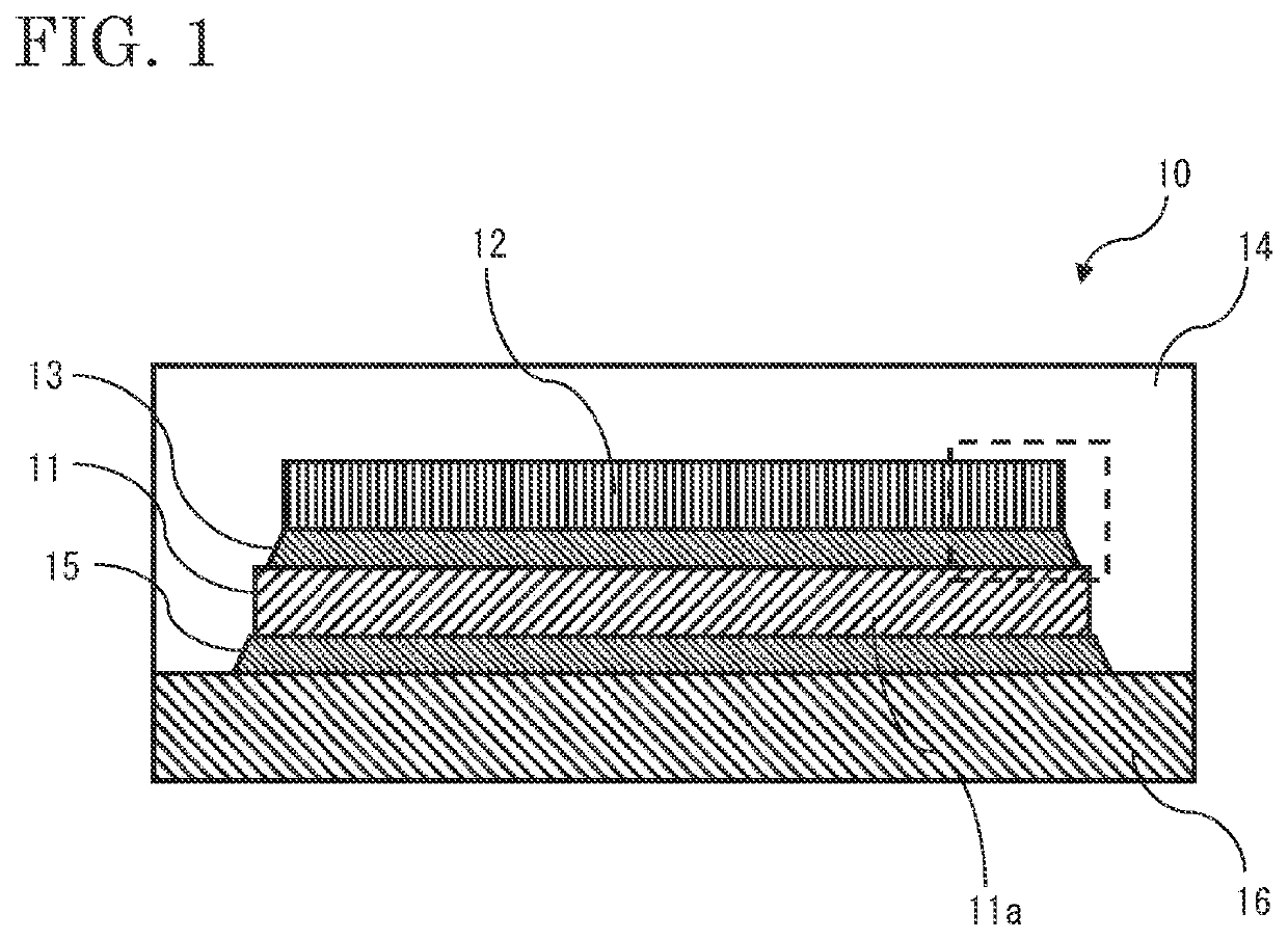
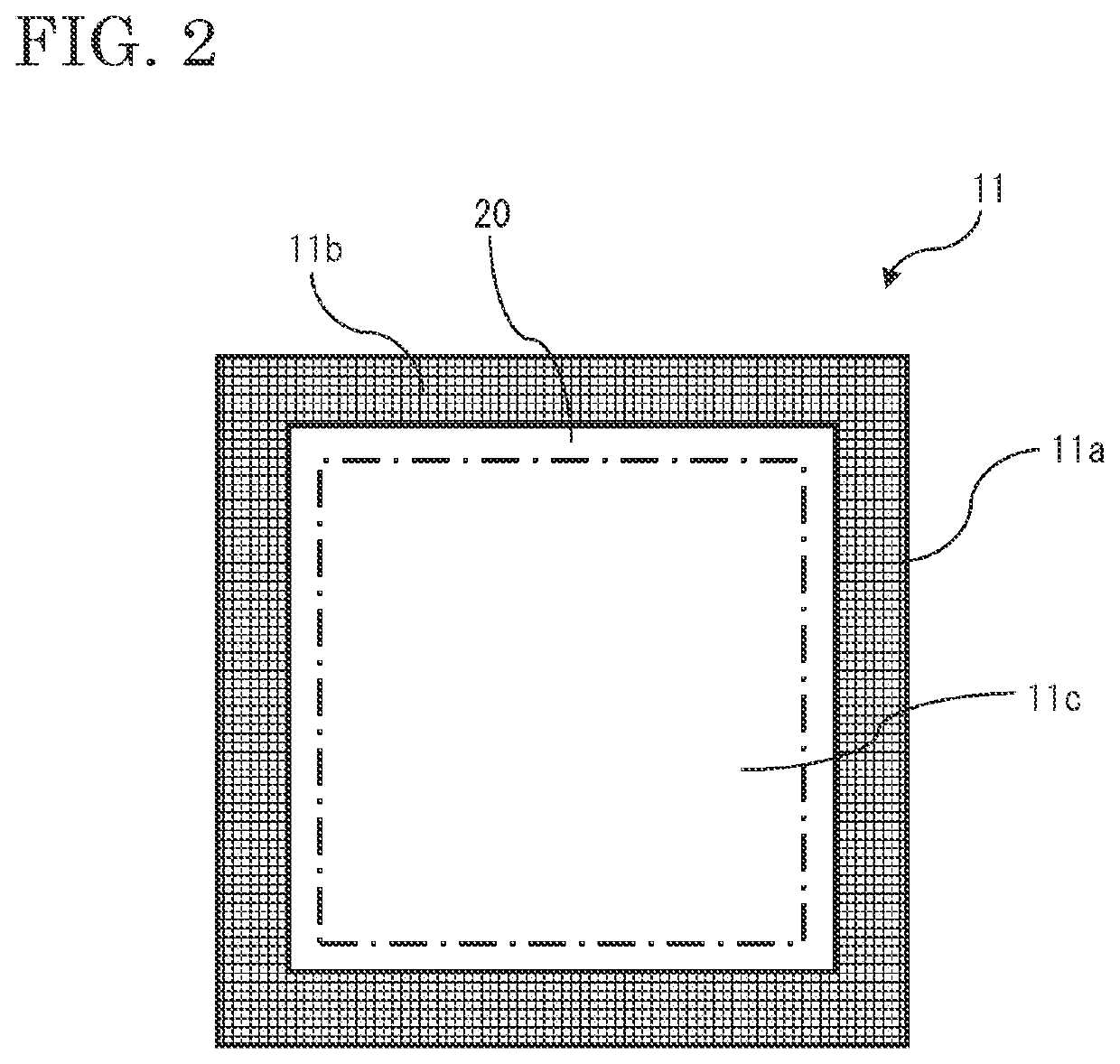
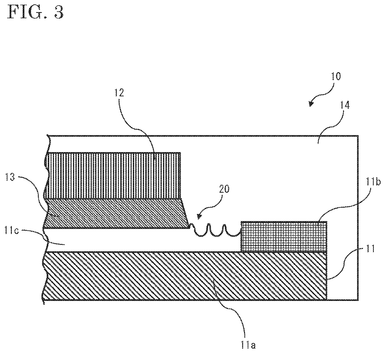
[0021]FIG. 1 is a sectional view schematically showing a semiconductor device 10 according to the first embodiment of the present disclosure, FIG. 2 is a plan view schematically showing a semiconductor element 11 of the semiconductor device 10, FIG. 3 is a sectional view showing a specific part of the semiconductor device 10, FIG. 4 is a plan view schematically showing another semiconductor element 11 of the semiconductor device 10, FIG. 5 is a sectional view showing a specific part of a semiconductor device 100 in Comparative example, and FIG. 6 is a flowchart showing a manufacturing process for the semiconductor device 10. The semiconductor device 10 is a device on which the semiconductor element 11 such as a semiconductor element for power control is mounted, and is used for a device for performing power conversion, or the like.
[0022]10>
[0023]The semiconductor device 10 includes the semiconductor element 11, a metal member 12, a heat spreader 16, solder 13 joining the semiconduct...
example
[0054]Hereinafter, the details of the present disclosure will be specifically described on the basis of Example and Comparative example. It is noted that the present disclosure is not limited thereto. FIG. 7 shows an evaluation result for the semiconductor device 10 in Example, and FIG. 8 is a sectional view showing a specific part regarding the evaluation result for the semiconductor device 10 in Example. The evaluation was conducted on three items: suppression of solder wetting, damage of the semiconductor element, and electric property.
[0055]
[0056]The semiconductor element 11 used in the evaluation described later will be described. The semiconductor element 11 is joined to the heat spreader 16 made of copper. The semiconductor element 11 is an IGBT. The metal thin film 11c on the surface of the semiconductor element 11 is a plating film mainly composed of nickel, and the thickness of the plating film is about 5 μm. At the outer periphery of the metal thin film 11c, the protectio...
PUM
 Abstract
Description
Claims
Application Information