Multiple bond via arrays of different wire heights on a same substrate

a multi-bonding, substrate technology, applied in the direction of microstructural technology, microstructured devices, inductances, etc., can solve problems such as solder bridging

Active Publication Date: 2015-12-31
INVENSAS CORP
View PDF4 Cites 21 Cited by
  • Summary
  • Abstract
  • Description
  • Claims
  • Application Information

AI Technical Summary

Problems solved by technology

Conventional interconnecting of an IC to another IC...

Method used


Image

  • Multiple bond via arrays of different wire heights on a same substrate
  • Multiple bond via arrays of different wire heights on a same substrate
  • Multiple bond via arrays of different wire heights on a same substrate

Examples


Embodiment Construction

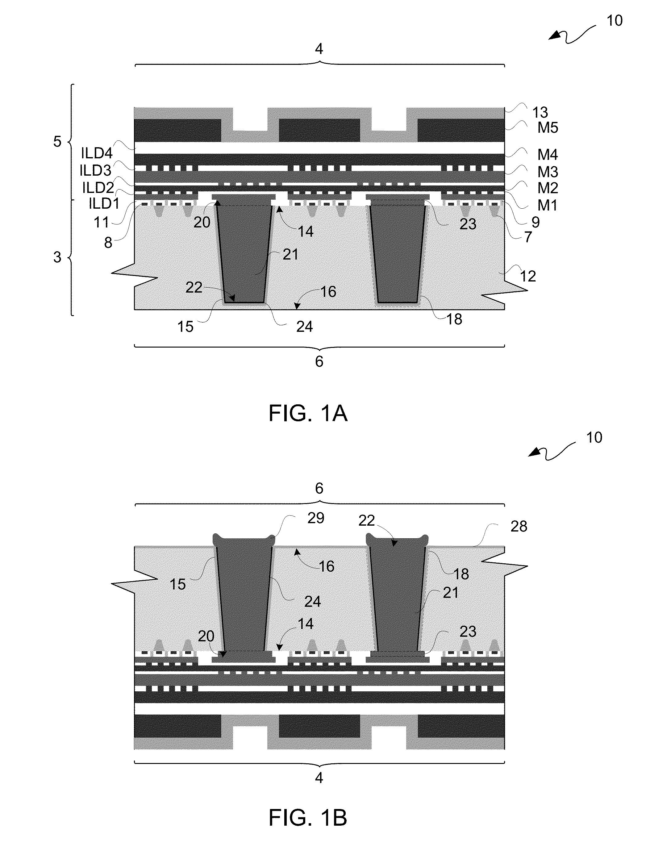
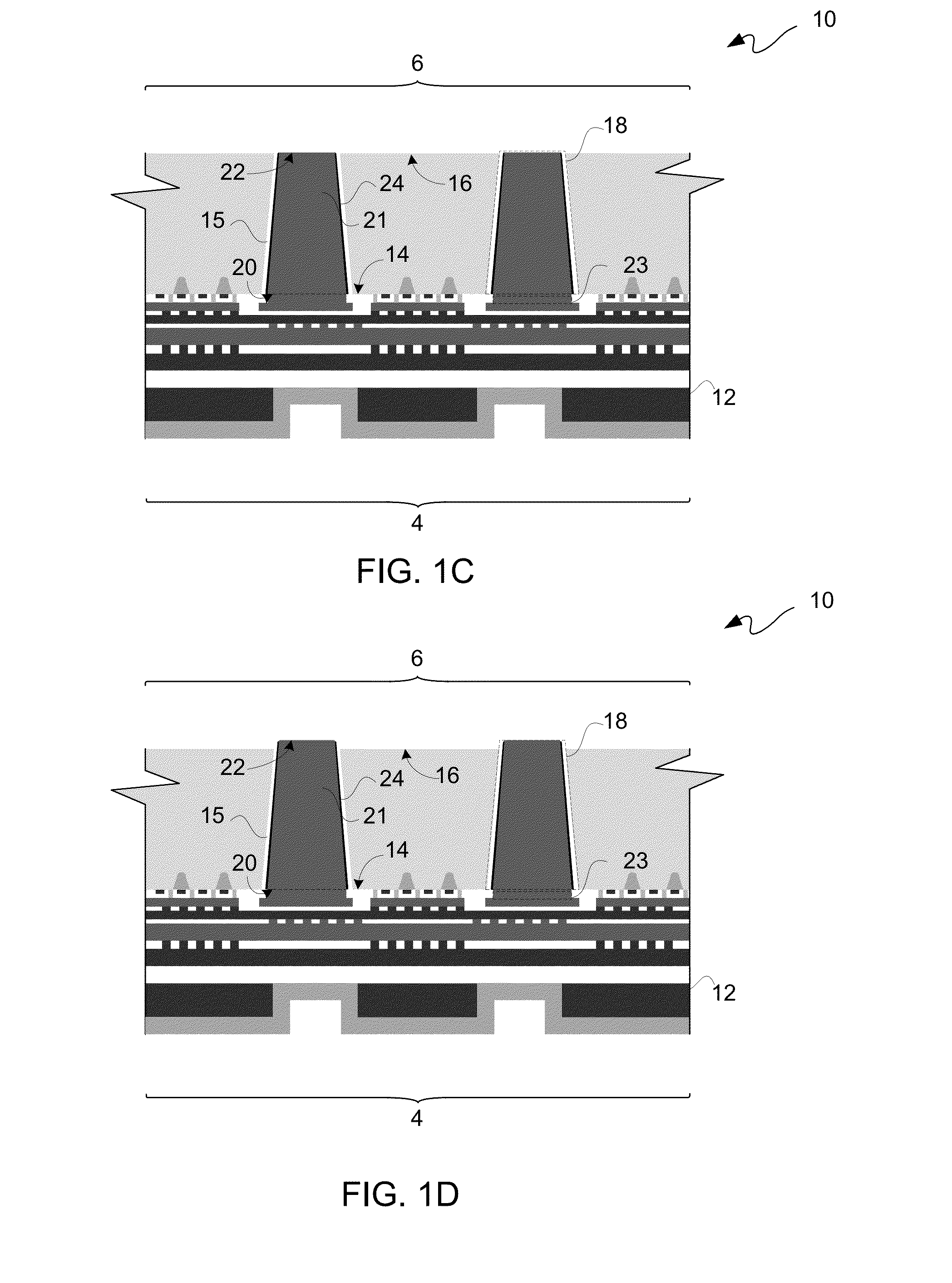
[0027]In the following description, numerous specific details are set forth to provide a more thorough description of the specific examples described herein. It should be apparent, however, to one skilled in the art, that one or more other examples or variations of these examples may be practiced without all the specific details given below. In other instances, well known features have not been described in detail so as not to obscure the description of the examples herein. For ease of illustration, the same number labels are used in different diagrams to refer to the same items; however, in alternative examples the items may be different.

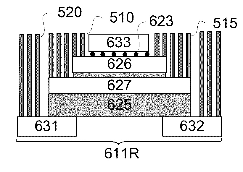
[0028]The following description generally relates to two or more bond via arrays (BVAs”) on a same surface of a substrate. At least two of these bond via arrays have wires of distinctly different heights for accommodation of die stacking within at least one of such bond via arrays and in some applications vias or wires may have different electrical...


PUM


Abstract

Apparatuses relating generally to a substrate are disclosed. In such an apparatus, first wire bond wires (“first wires”) extend from a surface of the substrate. Second wire bond wires (“second wires”) extend from the surface of the substrate. The first wires and the second wires are external to the substrate. The first wires are disposed at least partially within the second wires. The first wires are of a first height. The second wires are of a second height greater than the first height for coupling of at least one electronic component to the first wires at least partially disposed within the second wires.

Description

CROSS-REFERENCE TO RELATED APPLICATION(S)[0001]This application is a continuation-in-part of, and hereby claims priority to, pending U.S. patent application Ser. No. 14 / 087,252, filed on Nov. 22, 2013, the entirety of which is hereby incorporated by reference herein for all purposes.FIELD[0002]The following description relates to integrated circuits (“ICs”). More particularly, the following description relates to multiple bond via arrays of different wire heights on a same substrate for an IC package.BACKGROUND[0003]Microelectronic assemblies generally include one or more ICs, such as for example one or more packaged dies (“chips”) or one or more dies. One or more of such ICs may be mounted on a circuit platform, such as a wafer such as in wafer-level-packaging (“WLP”), printed board (“PB”), a printed wiring board (“PWB”), a printed circuit board (“PCB”), a printed wiring assembly (“PWA”), a printed circuit assembly (“PCA”), a package substrate, an interposer, or a chip carrier. Add...

Claims


Application Information

Patent Timeline
IPC IPC(8): H01L23/00H01L25/16
CPCH01L2225/06541H01L2225/06562H01L2224/48091H01L2224/45147H01L2224/45015H01L2924/00014H01L2225/06568H01L2225/06548H01L2224/16265H01L28/40H01L28/20H01L2924/1461B81B7/0074H01L2924/1207H01L2924/1206H01L2924/1205H01L28/10H01L24/45H01L2924/01074H01L2924/01082H01L2924/20751H01L2924/20752H01L2924/20753H01L2924/2076H01L2924/20755H01L2924/20756H01L2924/20757H01L2924/20758H01L2924/20759H01L2924/20754H01L25/0657H01L2224/0239H01L2224/0332H01L2224/0345H01L2224/03452H01L2224/03462H01L2224/03464H01L2224/1191H01L2224/13022H01L2224/13082H01L2224/131H01L2224/13111H01L2224/13113H01L2224/13116H01L2224/13124H01L2224/13139H01L2224/13144H01L2224/13147H01L2224/13155H01L2224/13169H01L2224/13184H01L2224/1403H01L2224/16145H01L2224/16146H01L2224/16148H01L2224/16225H01L2224/17181H01L2224/24227H01L2224/32145H01L2224/33181H01L2224/73253H01L2224/73265H01L2224/81192H01L2224/81193H01L2924/01322H01L2924/15192H01L2924/15311H01L2924/15787H01L2924/15788H01L2924/16251H01L2224/05568H01L2224/03912H01L2224/03914H01L2224/13616H01L2224/73201H01L2224/05565H01L2224/0333H01L23/3675H01L23/42H01L23/522H01L23/5383H01L24/94H01L25/0652H01L25/16H01L25/50H01L2224/13025H01L2224/94H01L2225/0651H01L2225/06517H01L2924/19041H01L2924/19042H01L2924/19043H01L2924/19103H01L2225/06513H01L2224/14131H01L2224/14134H01L24/97H01L2224/04042H01L2224/13023H01L2224/16227H01L2224/97H01L2224/14132H01L24/49H01L2224/4903H01L2924/3841H01L2224/0347H01L2224/0391H01L2224/0401H01L2224/05111H01L2224/05124H01L2224/05139H01L2224/05144H01L2224/05147H01L2224/05155H01L2224/05169H01L2224/05184H01L2224/05611H01L2224/05616H01L2224/05624H01L2224/05639H01L2224/05644H01L2224/05647H01L2224/05655H01L2224/05669H01L2224/05684H01L2224/1134H01L2224/11462H01L2224/11464H01L2224/1147H01L2224/11903H01L2224/05569H01L2224/05547H01L2224/3303H01L2224/244H01L2224/13565H01L2924/181H01L2224/03614H01L2224/81825H01L2924/12042H01L2224/24147H01L2224/48149H01L23/481H01L23/49811H01L21/4853H01L24/02H01L24/03H01L24/05H01L24/11H01L24/13H01L24/14H01L24/16H01L24/17H01L24/24H01L24/32H01L24/33H01L24/48H01L24/73H01L24/81H01L2924/00H01L2924/01029H01L2924/014H01L2924/00012H01L2924/01028H01L2224/05H01L2224/13H01L2224/81H01L2224/45099B81C1/0023H01L24/85H01L2224/8114
Inventor UZOH, CYPRIAN EMEKAKATKAR, RAJESH
Owner INVENSAS CORP
Why Eureka
Try Eureka