
E-fuse array circuit and semiconductor memory apparatus having the same

Inactive Publication Date: 2016-01-14
SK HYNIX INC
View PDF2 Cites 3 Cited by
  • Summary
  • Abstract
  • Description
  • Claims
  • Application Information

AI Technical Summary

Benefits of technology

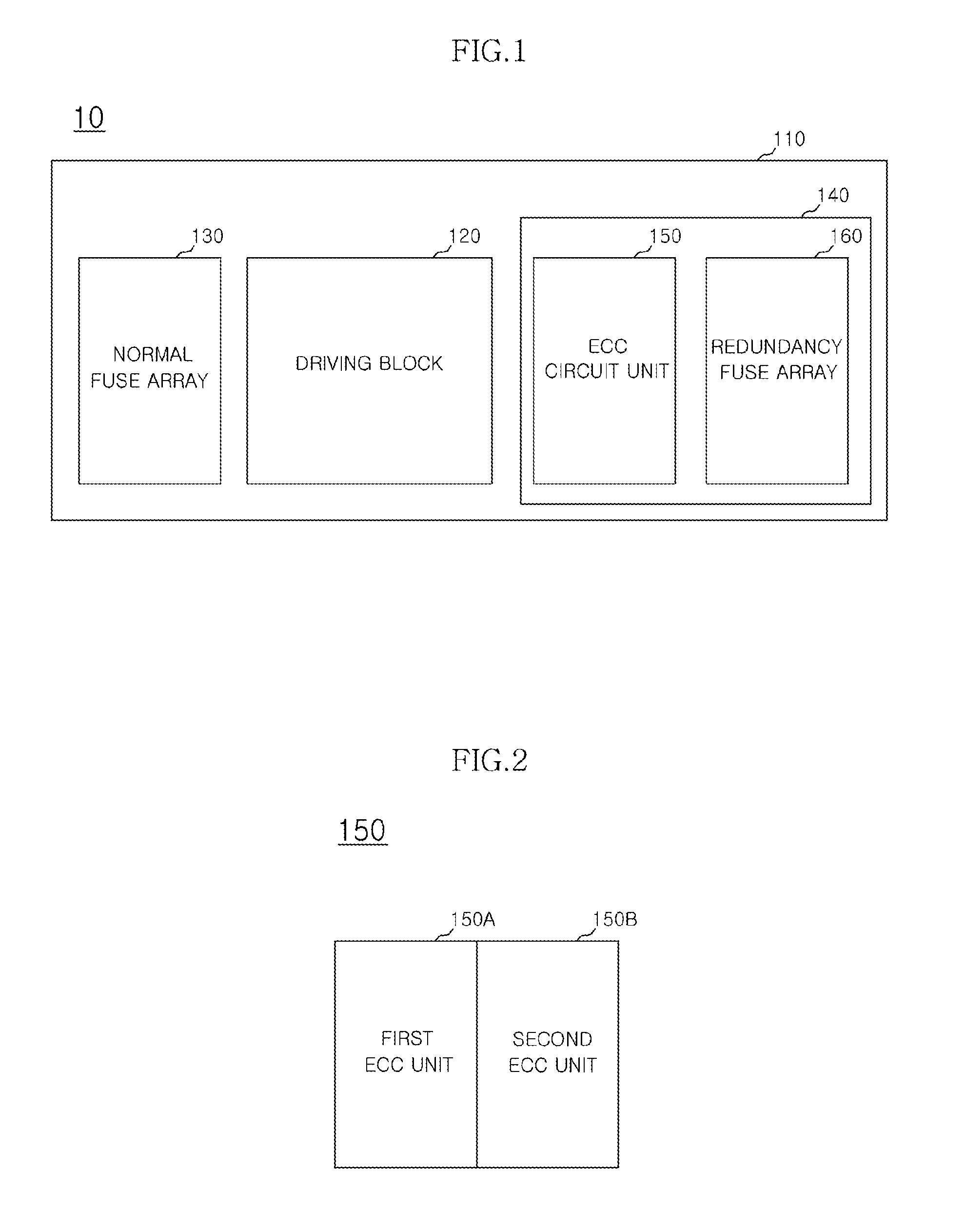
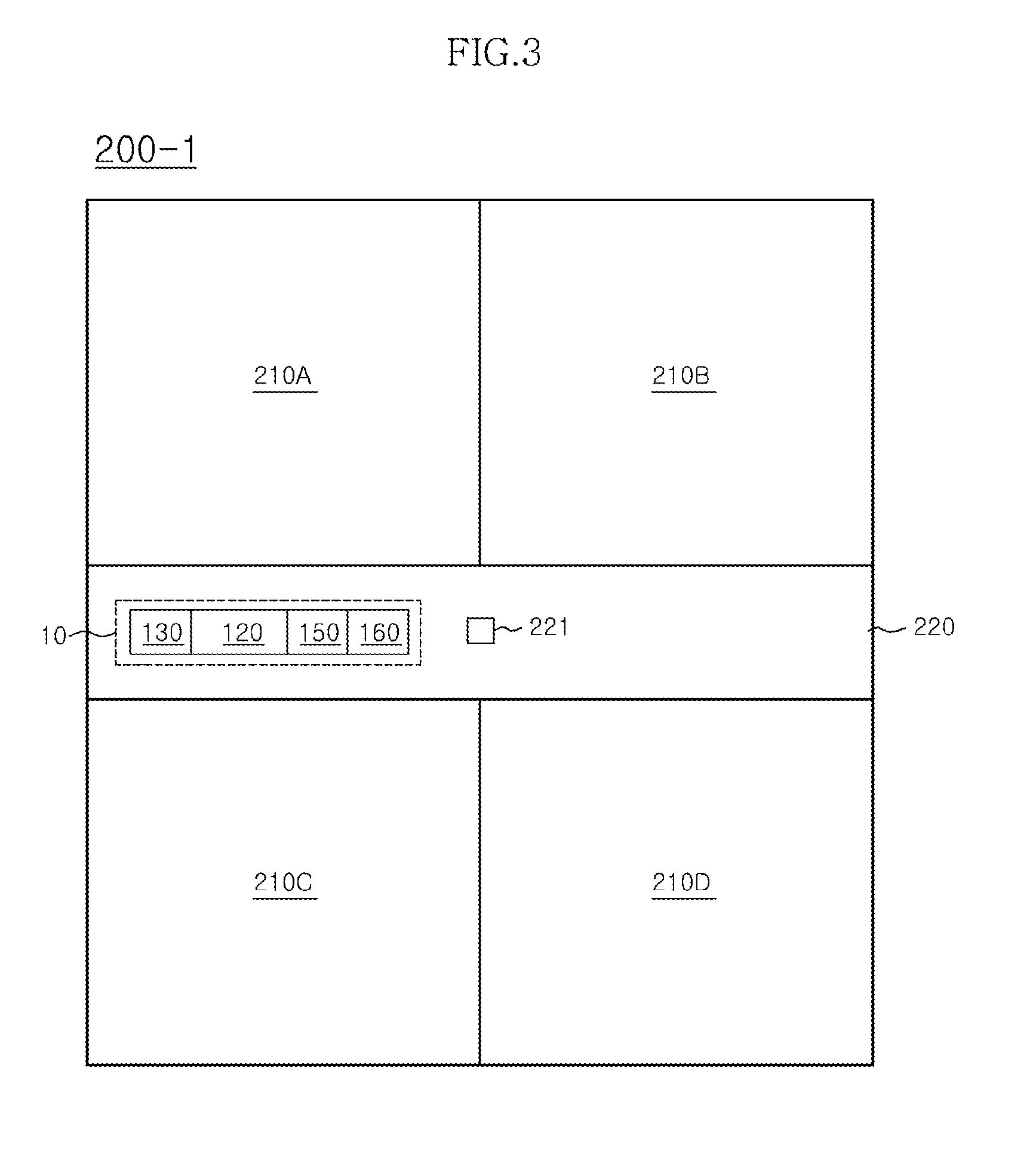
The patent text describes an E-fuse array circuit and a semiconductor memory apparatus that includes the circuit. The circuit includes a driving block, a normal fuse array, and an auxiliary circuit part. The driving block is arranged in a predetermined region on a semiconductor substrate and the normal fuse array is located close to one side of the driving block. The auxiliary circuit part is located on the other side of the driving block and facing the arrangement direction of the normal fuse array. The technical effect of this invention is to provide a more efficient and reliable E-fuse array circuit for use in semiconductor memory apparatuses.

Problems solved by technology

Therefore, it is possible to program the fuses on a wafer level, but it is impossible to program the fuses after packaging.
However, a voltage having a high level to which a transistor is not endurable is applied to the gate terminal, a gate oxide of the transistor is broken, and the gate terminal and the drain / source terminal are short-circuited.

Method used


Image

  • E-fuse array circuit and semiconductor memory apparatus having the same
  • E-fuse array circuit and semiconductor memory apparatus having the same
  • E-fuse array circuit and semiconductor memory apparatus having the same

Examples


Embodiment Construction

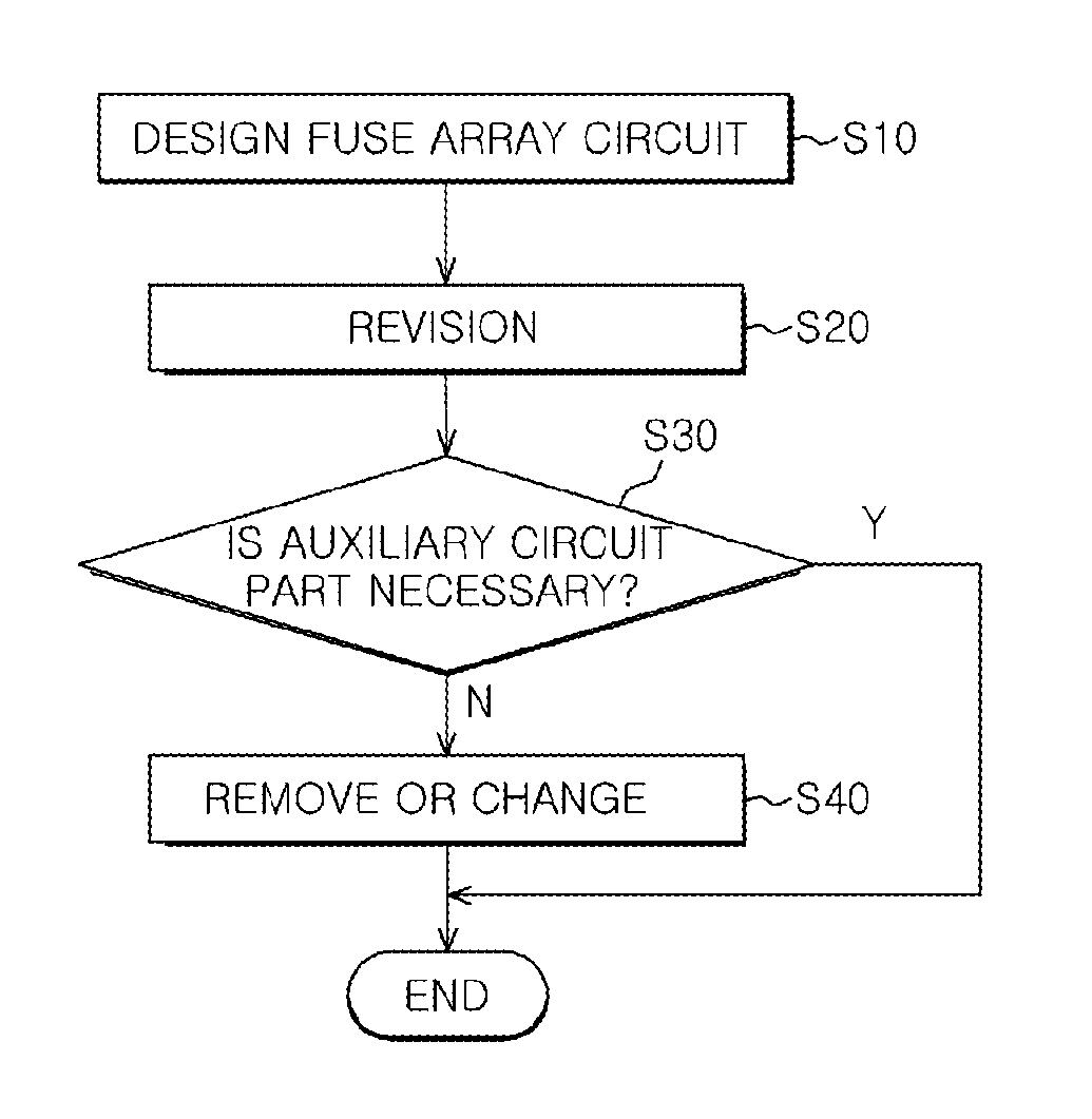
[0019]Various embodiments will be described in greater detail with reference to the accompanying drawings. Various embodiments are described with reference to cross-sectional illustrations that are schematic illustrations of various embodiments (and intermediate structures). As such, variations from the shapes of the illustrations as a result, for example, of manufacturing techniques and / or tolerances, are to be expected. Thus, embodiments should not be construed as limited to the particular shapes of regions illustrated but may include deviations in shapes that result, for example, from manufacturing. In the drawings, lengths and sizes of layers and regions may be exaggerated for clarity. Like reference numerals in the drawings denote like elements. It is also understood that when a layer is referred to as being “on” another layer or substrate, it can be directly on the other or substrate, or intervening layers may also be present. It is also noted that in this specification, “conn...


PUM


Abstract

An E-fuse array circuit includes a driving block arranged in a predetermined portion of a semiconductor substrate, a normal fuse array configured to one side of the driving block, and an auxiliary circuit part arranged in an other side of the driving block to a direction facing an arrangement direction of the normal fuse array.

Description

CROSS-REFERENCES TO RELATED APPLICATION[0001]This application claims priority under 35 U.S.C. 119(a) to Korean application No. 10-2014-0086094, filed on Jul. 9, 2014, in the Korean intellectual Property Office, which is incorporated by reference in its entirety as set forth in full.BACKGROUND[0002]1. Technical Field[0003]Various embodiments of the inventive concept relate to a semiconductor integrated circuit device, and more particularly, to an electric fuse (E-fuse) array circuit and a semiconductor memory apparatus having the same.[0004]2. Related Art[0005]Fuses in metal fuses are cut by a laser. A programming state is classified according to the cutting of the fuse. Therefore, it is possible to program the fuses on a wafer level, but it is impossible to program the fuses after packaging.[0006]To overcome drawbacks of the metal fuses, E-fuses are developed. The E-fuses are fabricated in a transistor form, and data is stored by changing a resistance between a gate and a drain / sour...

Claims


Application Information

Patent Timeline
IPC IPC(8): G11C17/16G11C17/18G11C29/00G11C29/42
CPCG11C17/16G11C29/42G11C29/787G11C17/18G11C29/027G11C2029/0411
Inventor KANG, HYUK, CHOONG
Owner SK HYNIX INC
Learn More