Electrical connection device and electronic device having same

a technology which is applied in the field of electrical connection device and electronic device having same, can solve the problems of manufacturing costs, increasing the number of assembling processes, and increasing the electric shock of electronic device when charged, so as to improve the antenna performance and reduce the electric shock

Active Publication Date: 2016-01-21
SAMSUNG ELECTRONICS CO LTD
View PDF19 Cites 28 Cited by
  • Summary
  • Abstract
  • Description
  • Claims
  • Application Information

AI Technical Summary

Benefits of technology

[0005]According to various embodiments, when the outer appearance of an electronic device is made of a conductive material, a conductive frame enclosing a terminal and a conductive bracket are integrally configured, so that the conductive frame may be used as an antenna. At this time, the conductive frame is electrically connected to a ground of a PCB in order to improve a performance of an antenna. However, in the configuration, a substrate of the electronic device and the ground of the PCB are connected to each other, so that the conductive frame may cause electric shock when the electronic device is charged. According to various embodiments, in order to reduce electric shock, a DC ground is shorted and the AC ground is electrically connected.

Problems solved by technology

However, in the configuration, a substrate of the electronic device and the ground of the PCB are connected to each other, so that the conductive frame may cause electric shock when the electronic device is charged.
However, in such a configuration, a separate mounting space for the connecting body should be provided inside the electronic device, which goes against a recent trend in which an electronic device becomes slim, light, short, and small.
Further, since a separate structure for the ground should be provided, the number of assembling processes and manufacturing costs are increased.

Method used


Image

  • Electrical connection device and electronic device having same
  • Electrical connection device and electronic device having same
  • Electrical connection device and electronic device having same

Examples


Embodiment Construction

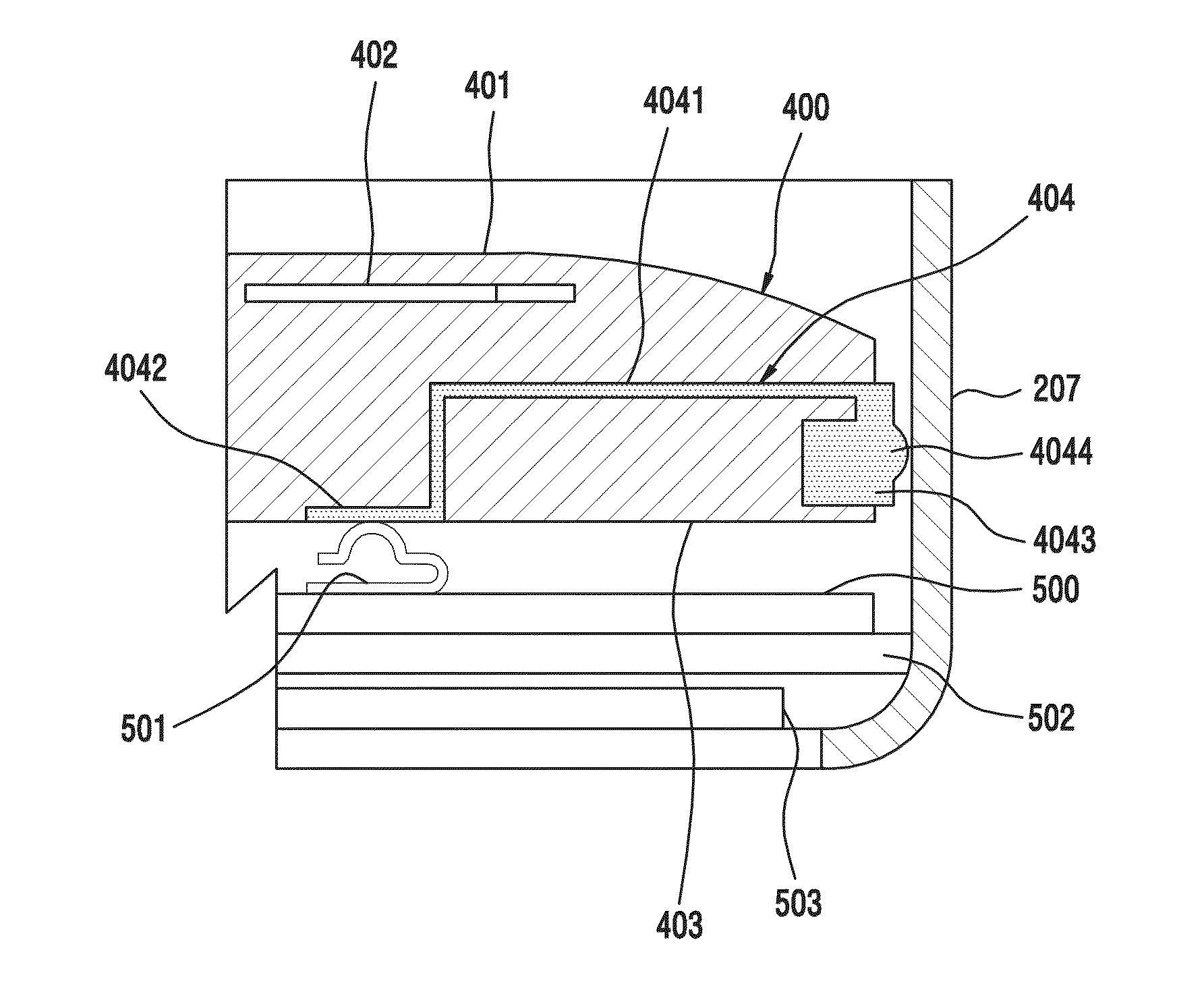
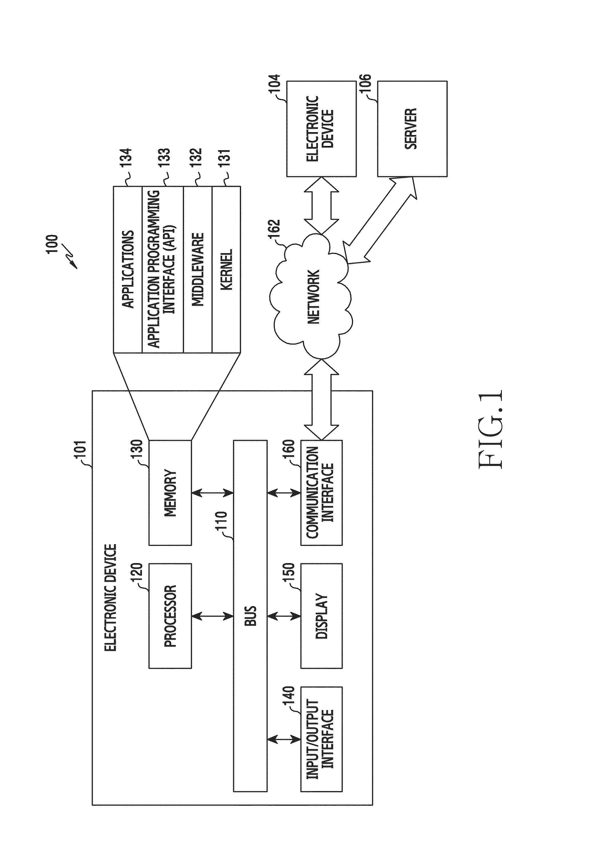
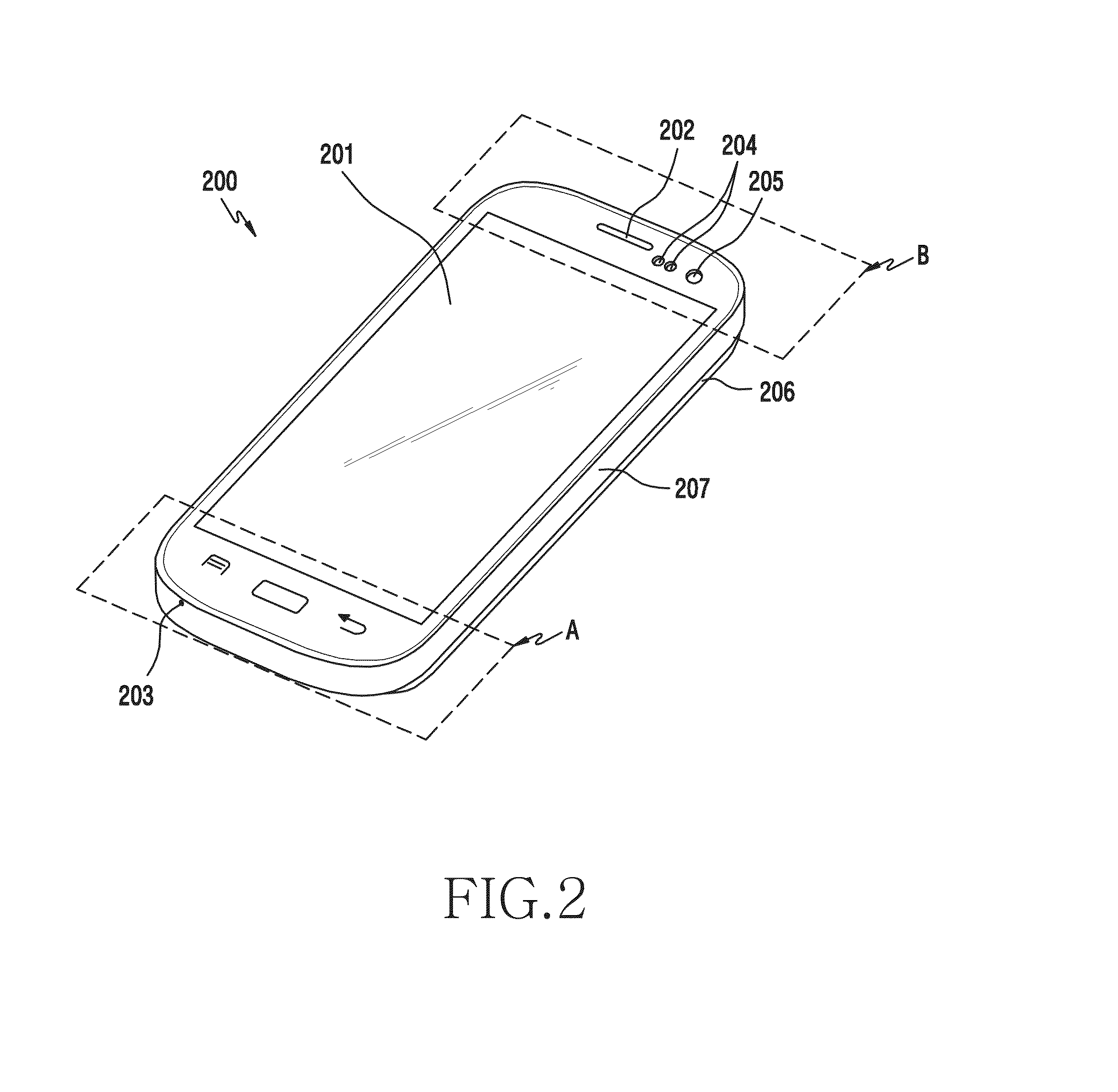
[0025]FIGS. 1 through 8, discussed below, and the various embodiments used to describe the principles of the present disclosure in this patent document are by way of illustration only and should not be construed in any way to limit the scope of the disclosure. Those skilled in the art will understand that the principles of the present disclosure may be implemented in any suitably arranged electronic devices. Hereinafter, various exemplary embodiments of the present disclosure are described with reference to the accompanying drawings. While the various exemplary embodiments of the present disclosure are susceptible to various modifications and alternative forms, a specific embodiment thereof has been shown by way of example in the drawings and will herein be described in detail. It should be understood, however, that it is not intended to limit the various exemplary embodiments of the present disclosure to the particular form disclosed, but, on the contrary, the various exemplary emb...


PUM


Abstract

An electronic device includes a substrate, a structure arranged near the substrate and includes at least one electronic component, a conductive structure provided in the electronic device, and a conductor arranged in the structure, grounding the conductive structure to a ground of the substrate. Electronic components spaced within the electronic device are electrically connected to each other using the existing structure to be installed, so that a mounting space for preparing an electrical connector is prevented from being wasted, thereby making the electronic device slim. The embodiments according to the present disclosure can reduce the number of assembling processes and manufacturing costs.

Description

CROSS-REFERENCE TO RELATED APPLICATION AND CLAIM OF PRIORITY[0001]The present application is related to and claims benefit under 35 U.S.C. §119(a) to Korean Application Serial No. 10-2014-0090439, which was filed in the Korean Intellectual Property Office on Jul. 17, 2014, the entire content of which is hereby incorporated by reference.TECHNICAL FIELD[0002]Various embodiments of the present disclosure relate to an electronic device, e.g., an electronic device having an electrical connection device.BACKGROUND[0003]In recent, with the development of an electronic communication technology, electronic devices having various functions are appearing. These electronic devices generally have a convergence function for complexly performing one or more functions.[0004]In particular, in a trend in which a functional gap between electronic devices, which are recently released by various manufacturers, is being reduced remarkably, the electronic devices have slimmed gradually, have an increased ...

Claims


Application Information

Patent Timeline
Patent Type & Authority Applications(United States)
IPC IPC(8): G06F1/16
CPCG06F1/1698G06F1/1694G06F1/1688G06F1/1626H01Q1/243H01Q1/48H04M1/0277H05K9/0049H05K9/0064
Inventor HEO, JOONKIM, YONG-HWA
Owner SAMSUNG ELECTRONICS CO LTD
Why Eureka
Try Eureka