
Finfet with back-gate

a back-gate and finfet technology, applied in the field of microelectronics, can solve the problems of limiting the possibility of further reduction in dimensions, unable to place a second gate, and the trend of reducing the dimensions of microelectronic components such as integrated transistors, and achieves the effect of higher mechanical stability

Inactive Publication Date: 2016-01-21
S O I TEC SILICON ON INSULATOR THECHNOLOGIES
View PDF3 Cites 2 Cited by
  • Summary
  • Abstract
  • Description
  • Claims
  • Application Information

AI Technical Summary

Benefits of technology

The patent text describes a design for a channel that has two fins. This design allows for the benefits of both the front and back-gate to affect the channel. The presence of the back-gate also makes the fins stronger and more stable mechanically. This means that a stress engineer can have more control over the stress of the fins to optimize their performance.

Problems solved by technology

Recently, the trend of reducing dimensions in microelectronic components, such as integrated transistors, has become increasingly more difficult.
The standard CMOS architecture has reached critical dimensions, at which effect, which were before negligible, are now limiting the possibility of further reduction in the dimensions.
Unfortunately, since the finFET already has a gate placed on the two sides of the channel, the placement of a second gate has not been possible.

Method used


Image

  • Finfet with back-gate
  • Finfet with back-gate
  • Finfet with back-gate

Examples


Embodiment Construction

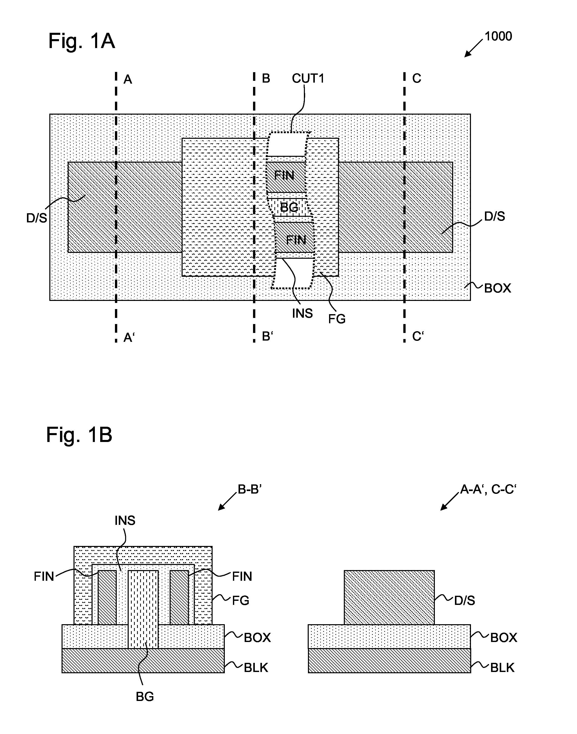
[0048]In particular, FIG. 1A schematically illustrates a top view of double-gate finFET 1000 while FIG. 1B schematically illustrates two cross-sections of double-gate finFET 1000 taken along lines B-B′, on the left part of FIG. 1B and taken along any of lines A-A′ and C-C′, on the right part of FIG. 1B. Moreover, FIG. 1A has an opening CUT1, allowing layers below the front-gate FG to be seen, for ease of understanding. It will be appreciated that in FIGS. 1A and 1B, as well as in the remaining figures described below, only the most relevant layers are illustrated. It is well understood by those skilled in the art that additional metal connections and / or via(s), for instance, will be necessary in order to connect the double-gate finFET 1000 to other elements. Similarly, it is clear that several layers, such as photoresists, will be necessary for the various manufacturing steps. Still additionally, it is obvious that the final circuit may comprise filling inert layers surrounding the ...


PUM


Abstract

The present invention relates to a double-gate finFET comprising: at least two fins (FIN) realizing a single channel; a back-gate (BG) placed between the fins; and a front-gate (FG), placed outside of the fins. Further, the invention relates to a manufacturing process, resulting in the double-gate finFET.

Description

CROSS-REFERENCE TO RELATED APPLICATIONS[0001]This application is a national phase entry under 35 U.S.C. §371 of International Patent Application PCT / EP2014 / 055039, filed Mar. 13, 2014, designating the United States of America and published in English as International Patent Publication WO 2014 / 146976 A1 on Sep. 25, 2014, which claims the benefit under Article 8 of the Patent Cooperation Treaty and under 35 U.S.C. §119(e) to France Patent Application Serial No. 1352466, filed Mar. 19, 2013, the disclosure of each of which is hereby incorporated herein in its entirety by this reference.TECHNICAL FIELD[0002]The present invention relates to the field of microelectronic. More specifically, it relates to a finFET which has two gates acting on its channel.BACKGROUND[0003]Recently, the trend of reducing dimensions in microelectronic components, such as integrated transistors, has become increasingly more difficult. The standard CMOS architecture has reached critical dimensions, at which eff...

Claims


Application Information

Patent Timeline
IPC IPC(8): H01L29/78H01L21/306H01L21/308H01L29/66
CPCH01L29/7855H01L29/7843H01L29/66484H01L21/308H01L29/66795H01L21/30604H01L29/7845
Inventor MAZURE, CARLOSHOFMANN, FRANZ
Owner S O I TEC SILICON ON INSULATOR THECHNOLOGIES
Learn More