Power Semiconductor Module

Active Publication Date: 2016-01-28
HITACHI ENERGY SWITZERLAND AG
View PDF0 Cites 0 Cited by
  • Summary
  • Abstract
  • Description
  • Claims
  • Application Information

AI Technical Summary

Benefits of technology

[0011]In comparison with a second circular line that would lie within the first circular line, the embodiment according to the invention leads to a delayed switching behavior of each power semiconductor component owing to the magnetic field being coupled into the conductor

Problems solved by technology

In the case of the known power semiconductor modules, it proves to be disadvantageous that, on account of the magnetic field that generates a current flow through the power semiconductor modules, the power semiconductor components arranged in the power semiconductor modu

Method used


Image

  • Power Semiconductor Module
  • Power Semiconductor Module
  • Power Semiconductor Module

Examples


Example

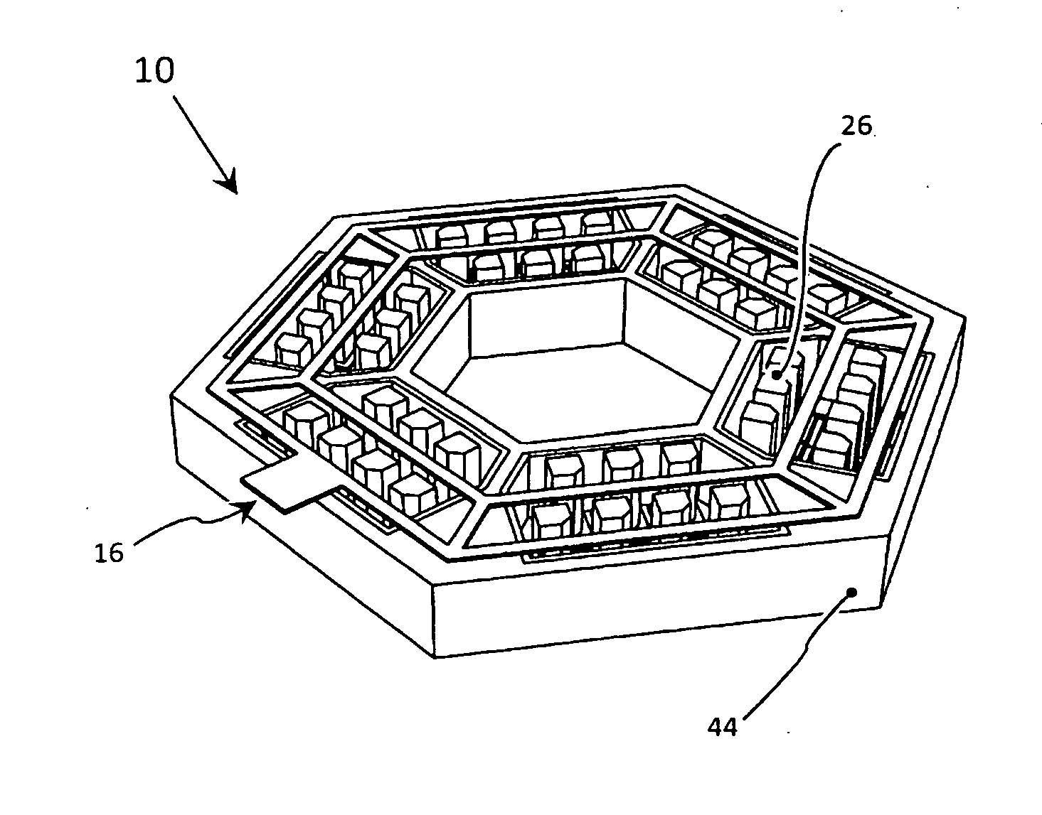
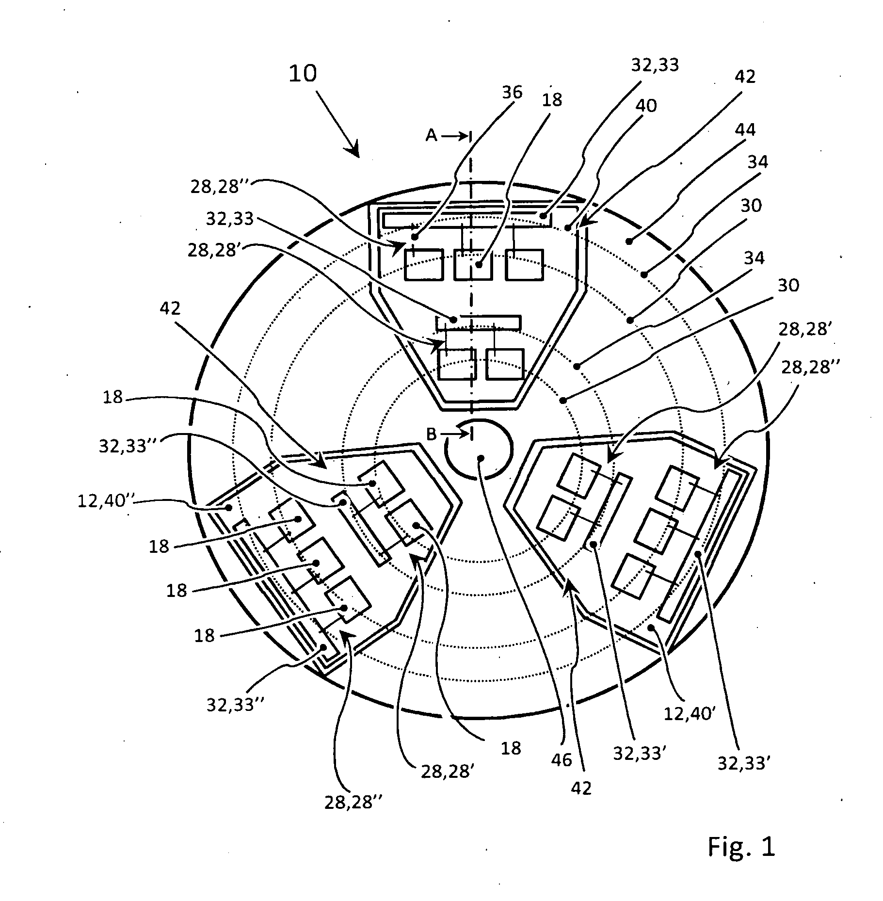
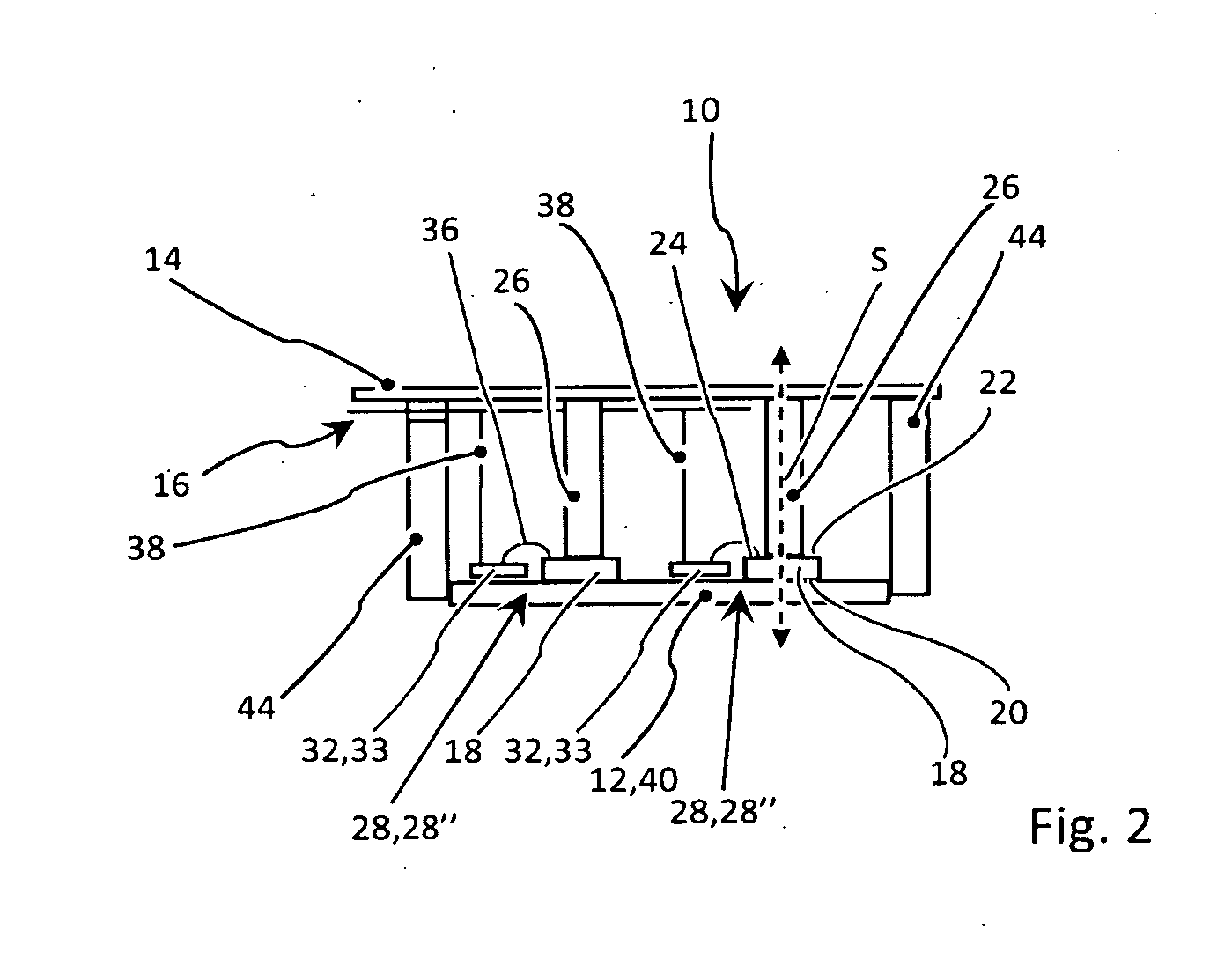
[0044]FIG. 1 and FIG. 2 show a first embodiment of a power semiconductor module 10 comprising a first main electrode 12 and a second main electrode 14, which is shown only in FIG. 2. The power semiconductor module 10 furthermore comprises a control terminal 16, shown in FIG. 2, which is arranged on the second main electrode 14 in a manner insulated from the second main electrode 14 in a known way. As shown in FIG. 2, in particular, controllable power semiconductor components 18 are arranged between the first main electrode 12 and the second main electrode 14. Each controllable power semiconductor component 18 has a first electrode 20, a second electrode 22 and a control electrode 24. The first electrode 20 of each controllable power semiconductor component 18 is electrically connected to the first main electrode 12 by means of a connection layer. The connection layer can be formed, for example, by a solder layer or by a connection layer produced by means of a sintering method. The s...


PUM


Abstract

A power semiconductor module includes a first main electrode, a second main electrode and a control terminal. The power semiconductor module includes controllable power semiconductor components arranged between the first main electrode and the second main electrode. At least some of the controllable power semiconductor components are arranged in a ring arrangement, wherein the controllable power semiconductor components of the ring arrangement are arranged at least approximately along a first circular line of the ring arrangement, and a control conductor track of the ring arrangement is arranged on the first main electrode, wherein the control conductor track runs at least approximately along a second circular line of the ring arrangement, and the second circular line runs concentrically relative to the first circular line.

Description

FIELD OF THE INVENTION[0001]The present invention relates to a power semiconductor module according to the invention.BACKGROUND OF THE INVENTION[0002]A power semiconductor module of this type is known from DE 196 44 009 A1.[0003]Further power semiconductor modules are also likewise known from the prior art and described for example in EP 0 989 611 A2, U.S. Pat. No. 6,426,561, EP 1 403 923 A1 or WO 2012 / 107482 A2. These modules are used for example for power converter installations for high voltage direct current transmission. A power semiconductor module is typically loaded minimally with more than 500 V and with more than 1 kA during operation. When the power semiconductor modules are employed in a power converter installation for high voltage direct current transmission, the power semiconductor modules are connected in series in order to achieve the required blocking voltage.[0004]Between 100 and 1000 power semiconductor modules are typically connected in series.[0005]Furthermore,...

Claims


Application Information

Patent Timeline
IPC IPC(8): H01L25/07H01L23/051H01L23/492
CPCH01L25/072H01L23/492H01L23/051H01L2224/48091H01L2924/13055H01L2924/00014H01L2924/00
Inventor HARTMANN, SAMUELDUGAL, FRANCEKWALL, OLLEDORE, ERIK
Owner HITACHI ENERGY SWITZERLAND AG
Why Eureka
Try Eureka