
Output Signal Generation Circuitry for Converting an Input Signal From a Source Voltage Domain Into an Output Signal for a Destination Voltage Domain

a technology of output signal and output signal, which is applied in the direction of logic circuit, electric pulse generator, power consumption reduction, etc., can solve the problems of timing delay, timing delay may be introduced between one end of tracking circuitry, and may not be acceptabl

Active Publication Date: 2016-02-04
ARM LTD
View PDF1 Cites 16 Cited by
  • Summary
  • Abstract
  • Description
  • Claims
  • Application Information

AI Technical Summary

Benefits of technology

The patent describes a method for converting signals from one voltage to another, while ensuring that the voltage drop across components in the circuit is below a certain threshold. This method also introduces a delay in the change of the output signal in response to changes in the input signal. The patent aims to provide a solution for this delay and to control the voltage on the output node accordingly. The technical effect of this patent is to improve the efficiency and reliability of signal conversion circuits, while ensuring that the components within the circuit are not stressed beyond their limits.

Problems solved by technology

The technical problem addressed in this patent text is to provide an improved level shifter that can convert signals in one voltage domain into a form suitable for another voltage domain without causing damage to the components due to overstress and without introducing significant timing delays that may affect the performance of the circuit.

Method used


Image

  • Output Signal Generation Circuitry for Converting an Input Signal From a Source Voltage Domain Into an Output Signal for a Destination Voltage Domain
  • Output Signal Generation Circuitry for Converting an Input Signal From a Source Voltage Domain Into an Output Signal for a Destination Voltage Domain
  • Output Signal Generation Circuitry for Converting an Input Signal From a Source Voltage Domain Into an Output Signal for a Destination Voltage Domain

Examples


Embodiment Construction

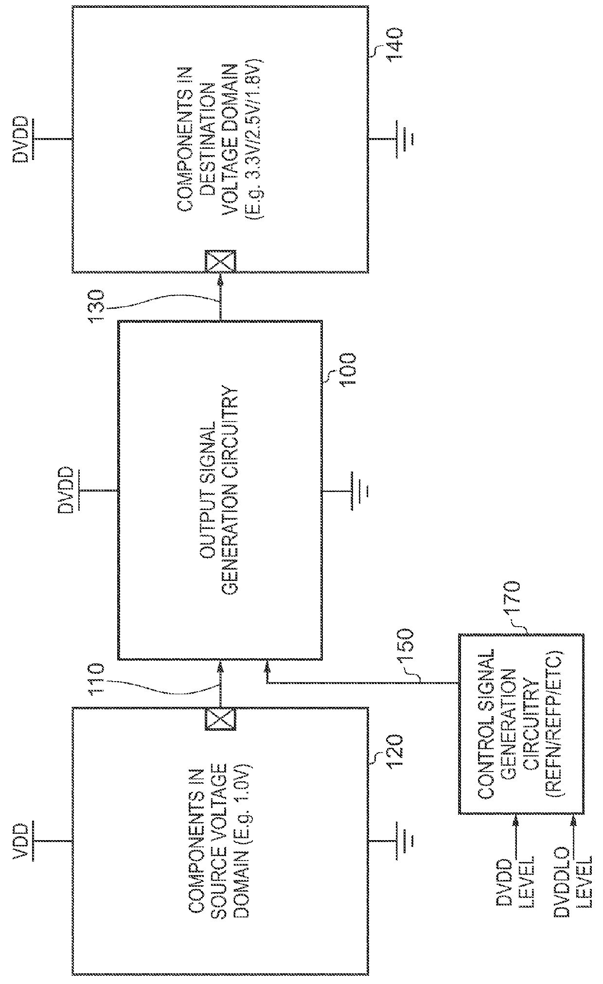
[0030]FIG. 1 shows the use of output signal generation circuitry 100. The output signal generation circuitry 100 takes, as an input, a signal 110 from components in a source voltage domain 120. The components in the source voltage domain 120 may operate between a supply voltage (VDD) of, for example, 1.0V and ground. The output signal generation circuitry 100 may then generate an output signal 130 for components in a destination voltage domain 140. The components in the destination voltage domain 140 may operate between a different supply voltage (DVDD) and ground. For example, the components in the destination voltage domain 140 may operate with a supply voltage of 3.3V, 2.5V or 1.8V, depending on the operating mode of those components. In this example, the output signal generation circuitry 100 operates using the supply voltage of the destination voltage domain. In other words, the output signal generation circuitry 100 operates between a supply voltage DVDD and ground. The output...


PUM


Abstract

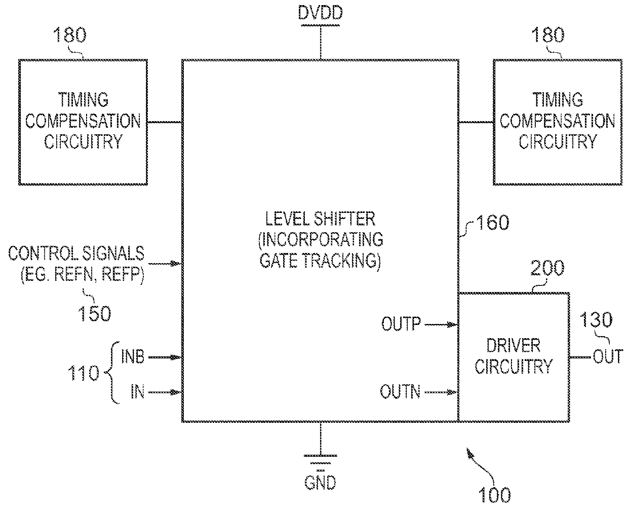
Output signal generation circuitry 100 may be used for converting an input signal 110 from a source voltage domain to an output signal for a destination voltage domain, the destination voltage domain operating from a supply voltage that exceeds a stressing threshold of components within the output signal generation circuitry. The output signal generation circuitry may comprise level shifting circuitry 160 operating from the supply voltage, which is configured to generate at an output node 130 the output signal for the destination voltage domain in dependence on the input signal. The output signal generation circuitry may also comprise tracking circuitry 280A, 280B, 280C, 280D associated with at least one component of the level shifting circuitry to ensure that a voltage drop across the at least one component does not exceed the stressing threshold, wherein the tracking circuitry additionally introduces a delay in a change in the output signal in response to a change in the input signal. Timing compensation circuitry 180A, 180B may also be provided, to control the voltage on the output node in a manner to compensate for the delay introduced by the tracking circuitry.

Description


Claims


Application Information

Patent Timeline
Owner ARM LTD
Learn More