Depletion-mode field effect transistor based electrostatic discharge protection circuit

Inactive Publication Date: 2011-02-01
QORVO US INC
View PDF10 Cites 37 Cited by
  • Summary
  • Abstract
  • Description
  • Claims
  • Application Information

AI Technical Summary

Benefits of technology

The present invention relates to an electrostatic discharge (ESD) clamp circuit that is used to protect other circuitry from high voltage ESD events. The ESD clamp circuit may include a field effect transistor (FET) element as a clamping element, which is triggered by using a drain-to-gate capacitance and a drain-to-gate resistance of the FET element and a resistive element as a voltage divider to divide down an ESD voltage to provide a triggering gate voltage of the FET element. In

Problems solved by technology

Electrostatic discharge (ESD), which is a large subset of electrical overstress (EOS), is a major reliability issue in integrated circuits (ICs).
As semiconductor devices have scaled to smaller dimensions and ICs have become more complex, the potential for destructive ESD events has become more serious.
However, ESD protection circuitry for Gallium Arsenide pHEMT technology that is currently in use may p

Method used


Image

  • Depletion-mode field effect transistor based electrostatic discharge protection circuit
  • Depletion-mode field effect transistor based electrostatic discharge protection circuit
  • Depletion-mode field effect transistor based electrostatic discharge protection circuit

Examples


first embodiment

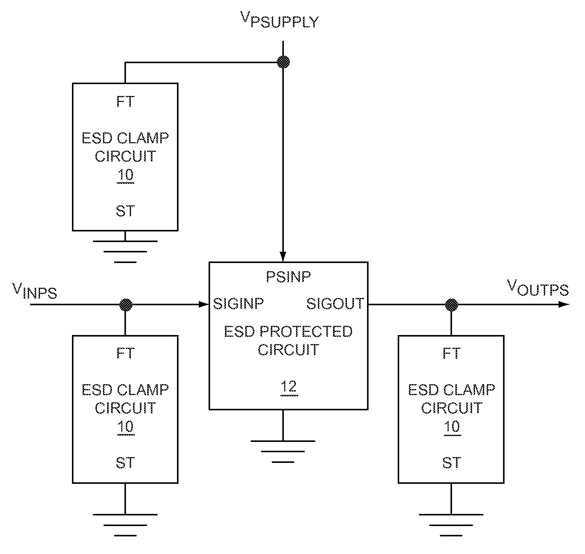
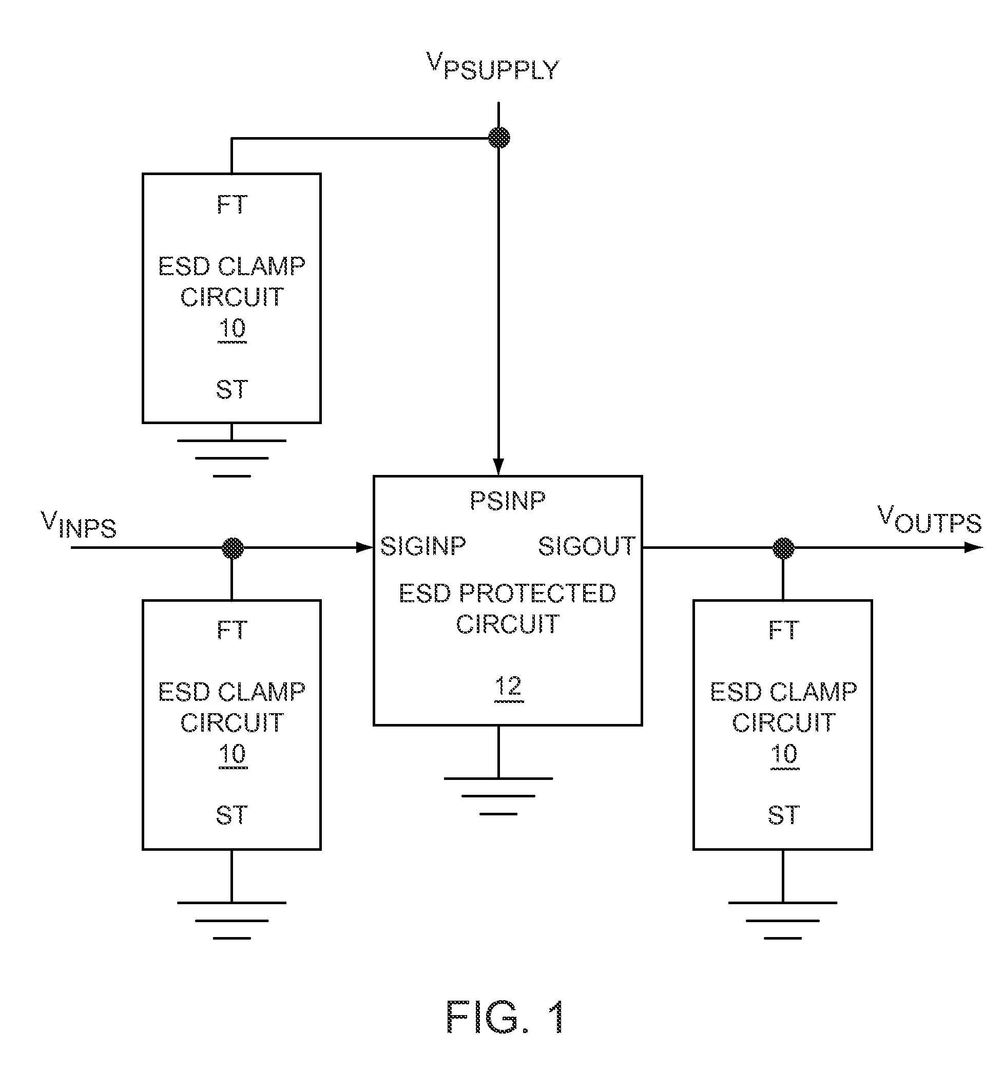
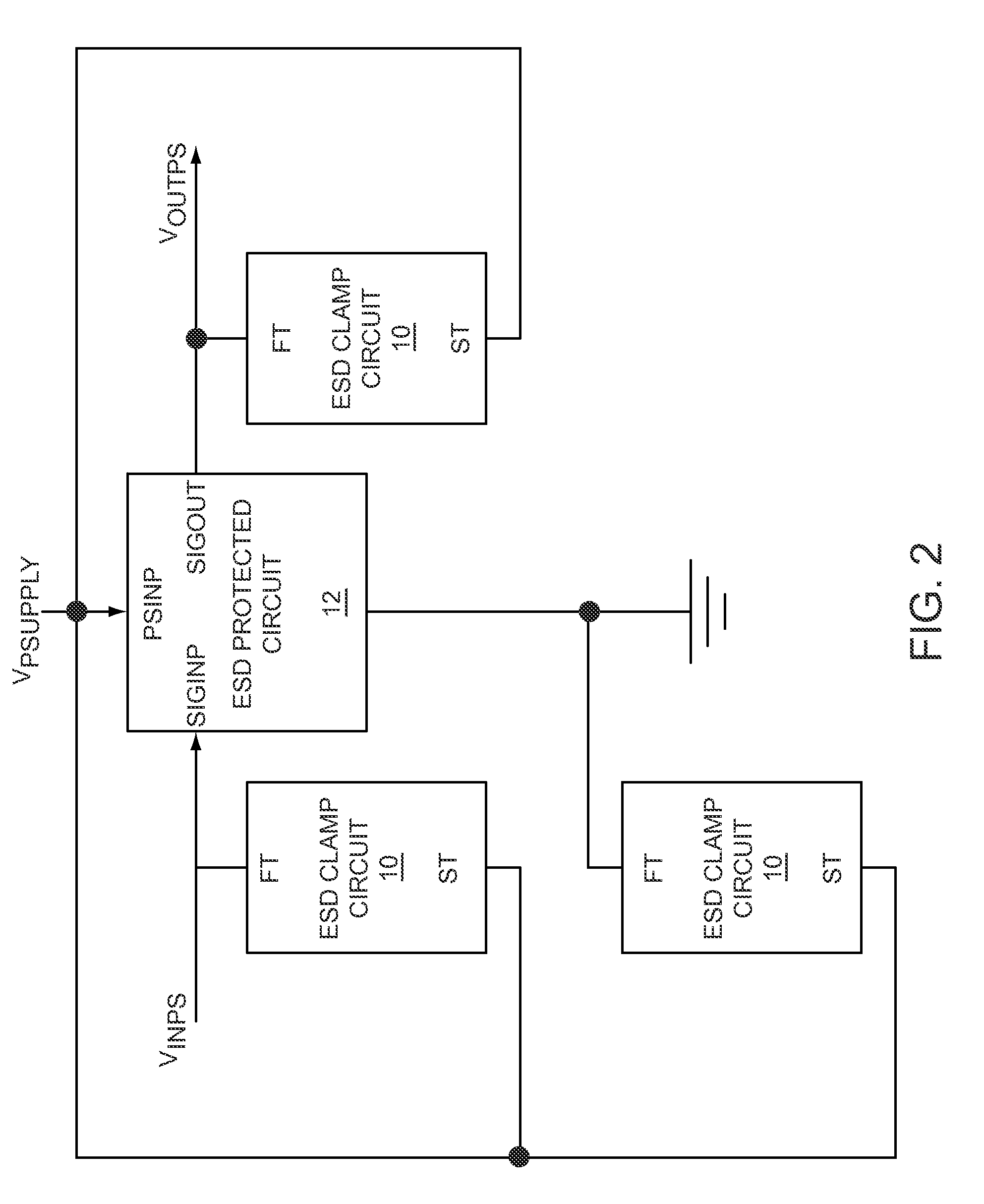
FIG. 5 shows details of the ESD clamp circuit, which includes a depletion-mode field effect transistor (FET) element, a first resistive element coupled between a gate and a source of the FET element, a source-coupled level shifting circuit, and a reverse protection circuit, according to the ESD clamp circuit.

second embodiment

FIG. 6 shows a series resistive element coupled in series with the depletion-mode FET element illustrated in FIG. 5, according to the ESD clamp circuit.

FIG. 7 shows details of the source-coupled level shifting circuit and the reverse protection circuit illustrated in FIG. 5, according to one embodiment of the ESD clamp circuit.

FIG. 8 shows details of the source-coupled level shifting circuit and the reverse protection circuit illustrated in FIG. 6, according to another embodiment of the ESD clamp circuit.

third embodiment

FIG. 9 shows multiple depletion-mode FET elements coupled in series according to the ESD clamp circuit.


PUM


Abstract

The present invention relates to an electrostatic discharge (ESD) clamp circuit that is used to protect other circuitry from high voltage ESD events. The ESD clamp circuit may include a field effect transistor (FET) element as a clamping element, which is triggered by using a drain-to-gate capacitance and a drain-to-gate resistance of the FET element and a resistive element as a voltage divider to divide down an ESD voltage to provide a triggering gate voltage of the FET element. In its simplest embodiment, the ESD clamp circuit includes only an FET element, a resistive element, a source-coupled level shifting diode, and a reverse protection diode. Therefore, the ESD clamp circuit may be small compared to other ESD protection circuits. The simplicity of the ESD clamp circuit may minimize parasitic capacitances, thereby maximizing linearity of the ESD clamp circuit over a wide frequency range.

Description

CROSS-REFERENCE TO RELATED APPLICATIONSThis application is related to U.S. patent application Ser. No. 11 / 609,497 entitled ON-CHIP ESD PROTECTION CIRCUIT FOR RADIO FREQUENCY (RF) INTEGRATED CIRCUITS filed Dec. 12, 2006, the disclosure of which is hereby incorporated herein by reference in its entirety.FIELD OF THE INVENTIONThe present invention relates to electrostatic discharge (ESD) protection circuits, which may be used to protect other circuits from the high voltages associated with ESD events.BACKGROUND OF THE INVENTIONElectrostatic discharge (ESD), which is a large subset of electrical overstress (EOS), is a major reliability issue in integrated circuits (ICs). As semiconductor devices have scaled to smaller dimensions and ICs have become more complex, the potential for destructive ESD events has become more serious. More recently, there has been a tremendous demand for increasing the ESD robustness of Radio Frequency (RF) ICs, especially for wireless applications, such as han...

Claims


Application Information

Patent Timeline
IPC IPC(8): H02H3/22
CPCH01Q1/50H03F1/52H03F2200/441
Inventor LI, JASON YUXINWOHLMUTH, WALTER A.MUTHUKRISHNAN, SWAMINATHANIVERSEN, CHRISTIAN RYEPEACHEY, NATHANIEL
Owner QORVO US INC
Why Eureka
Try Eureka