Forming method of radio frequency switching device and radio frequency switching device

A technology of radio frequency switches and devices, which is applied to waveguide devices, electrical components, circuits, etc., can solve problems such as the increase of quality factor FOM, the increase of off capacitance Coff, and the deterioration of the performance of radio frequency switching devices, so as to improve performance, Reduce the effect of Coff

Active Publication Date: 2021-07-02
SHANGHAI HUAHONG GRACE SEMICON MFG CORP
View PDF4 Cites 0 Cited by
  • Summary
  • Abstract
  • Description
  • Claims
  • Application Information

AI Technical Summary

Problems solved by technology

[0004] For RF switching devices, it mainly includes source, drain and gate. Generally, parasitic capacitance will be generated between drain and gate, and at the same time, parasitic capacitance will also be generated between source and gate. Parasitic capacitance The presence of will lead to an increase in the off-capacitance Coff, which will lead to an increase in the quality factor FOM, making the performance of the RF switching device worse

Method used


Image

  • Forming method of radio frequency switching device and radio frequency switching device
  • Forming method of radio frequency switching device and radio frequency switching device
  • Forming method of radio frequency switching device and radio frequency switching device

Examples


Embodiment Construction

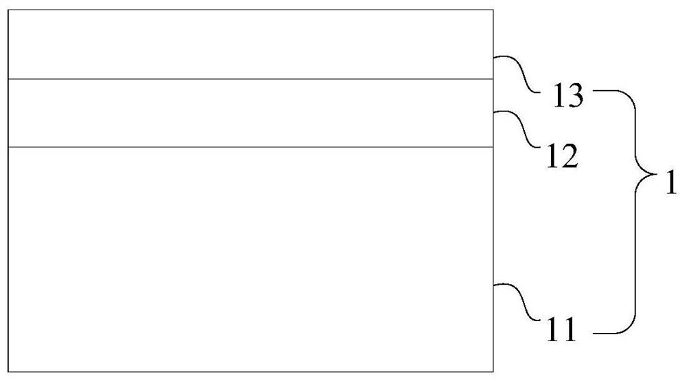
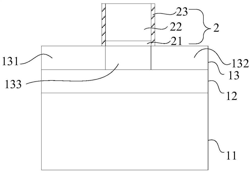
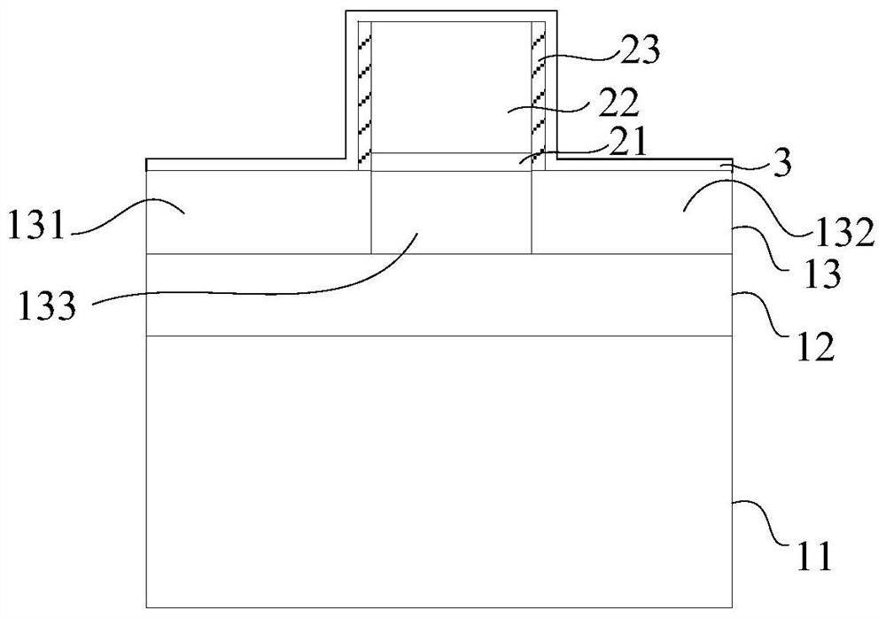
[0032] The method for forming the radio frequency switching device and the radio frequency switching device proposed by the present invention will be further described in detail below in conjunction with the accompanying drawings and specific embodiments. It should be noted that all the drawings are in a very simplified form and use imprecise scales, and are only used to facilitate and clearly assist the purpose of illustrating the embodiments of the present invention. In addition, the structures shown in the drawings are often a part of the actual structures. In particular, each drawing needs to display different emphases, and sometimes uses different scales.

[0033] The method for forming a radio frequency switching device provided in an embodiment of the present invention includes:

[0034] Step S10: providing a substrate;

[0035] Step S11: forming a gate structure on the substrate;

[0036] Step S12: forming an etching stop layer, the etching stop layer covering the g...


PUM

PropertyMeasurementUnit
widthaaaaaaaaaa
widthaaaaaaaaaa

Abstract

The invention provides a method for forming a radio frequency switching device and a radio frequency switching device, forming a gate structure on a substrate, and sequentially forming an etching stop layer, a first dielectric layer, a silicon nitride layer and a silicon nitride layer on the gate structure and the substrate. After the second dielectric layer, an air gap is formed in the silicon nitride layer. Since the air gap is relatively the lowest in dielectric constant, the existence of the air gap makes the final layer in the second dielectric layer Parasitic capacitances between the source metal layer formed on the second dielectric layer and the gate structure and between the drain metal layer formed on the second dielectric layer and the gate structure are minimized, thereby reducing the off-capacitance Coff, improving the performance of RF switching devices.

Description

technical field [0001] The invention relates to the technical field of semiconductor integrated circuit manufacturing, in particular to a method for forming a radio frequency switch device and the radio frequency switch device. Background technique [0002] The radio frequency switching device is a device used for signal switching in the communication field. It has the advantages of simple structure, wide application range, low cost, low power consumption, easy installation, and high reliability. It can be widely used in carrier telephone switching, cable television signal Switching, cable TV signal switch and other fields, when it is working, some areas are in the on state, and some areas are in the off state. [0003] The quality factor FOM (Figure Of Merit) is used to evaluate the switching performance or process capability of the field effect transistor MOSFET. It is a compromise between Insertion Loss and Isolation. The insertion loss is characterized by the on-resistan...

Claims


Application Information

Patent Timeline
Patent Type & Authority Patents(China)
IPC IPC(8): H01P1/15H01P11/00
Inventor 刘张李
Owner SHANGHAI HUAHONG GRACE SEMICON MFG CORP
Why Eureka
Try Eureka