Dynamically biased wide swing level shifting circuit for high speed voltage protection input/outputs

a wide swing level and voltage protection technology, applied in logic circuits, electronic switching, pulse techniques, etc., can solve the problem of not being able to fully turn on transistors, and achieve the effect of speeding up the i/o operation of output buffers

Active Publication Date: 2006-05-30
GULA CONSULTING LLC
View PDF34 Cites 39 Cited by
  • Summary
  • Abstract
  • Description
  • Claims
  • Application Information

AI Technical Summary

Benefits of technology

[0012]Because of the delay introduced by the two inverters in series, the voltage conveyed by the PUB output changes nearly simultaneously with a change in the voltage controlling the second transistor. In so doing, less dynamic stress is realized at the gate of the second transistor. Additionally, the voltage conveyed by the PUB output is significantly lower than in conventional level shifting circuits. As a result, more pullup current is allowed to pass from the output stage and the speed of I / O operations of the output buffer are achieved.

Problems solved by technology

This is an important challenge in input / output (I / )O design.
However, this voltage level is not low enough to fully turn on transistor 111 which is controlled by PUB 131.

Method used


Image

  • Dynamically biased wide swing level shifting circuit for high speed voltage protection input/outputs
  • Dynamically biased wide swing level shifting circuit for high speed voltage protection input/outputs
  • Dynamically biased wide swing level shifting circuit for high speed voltage protection input/outputs

Examples


Embodiment Construction

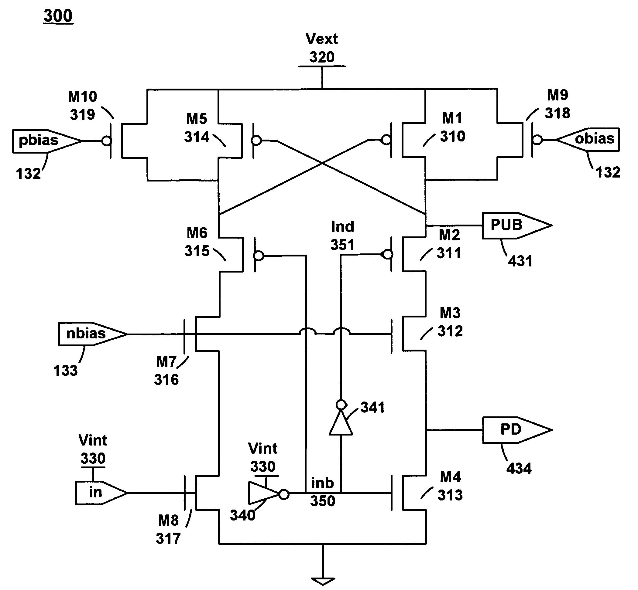
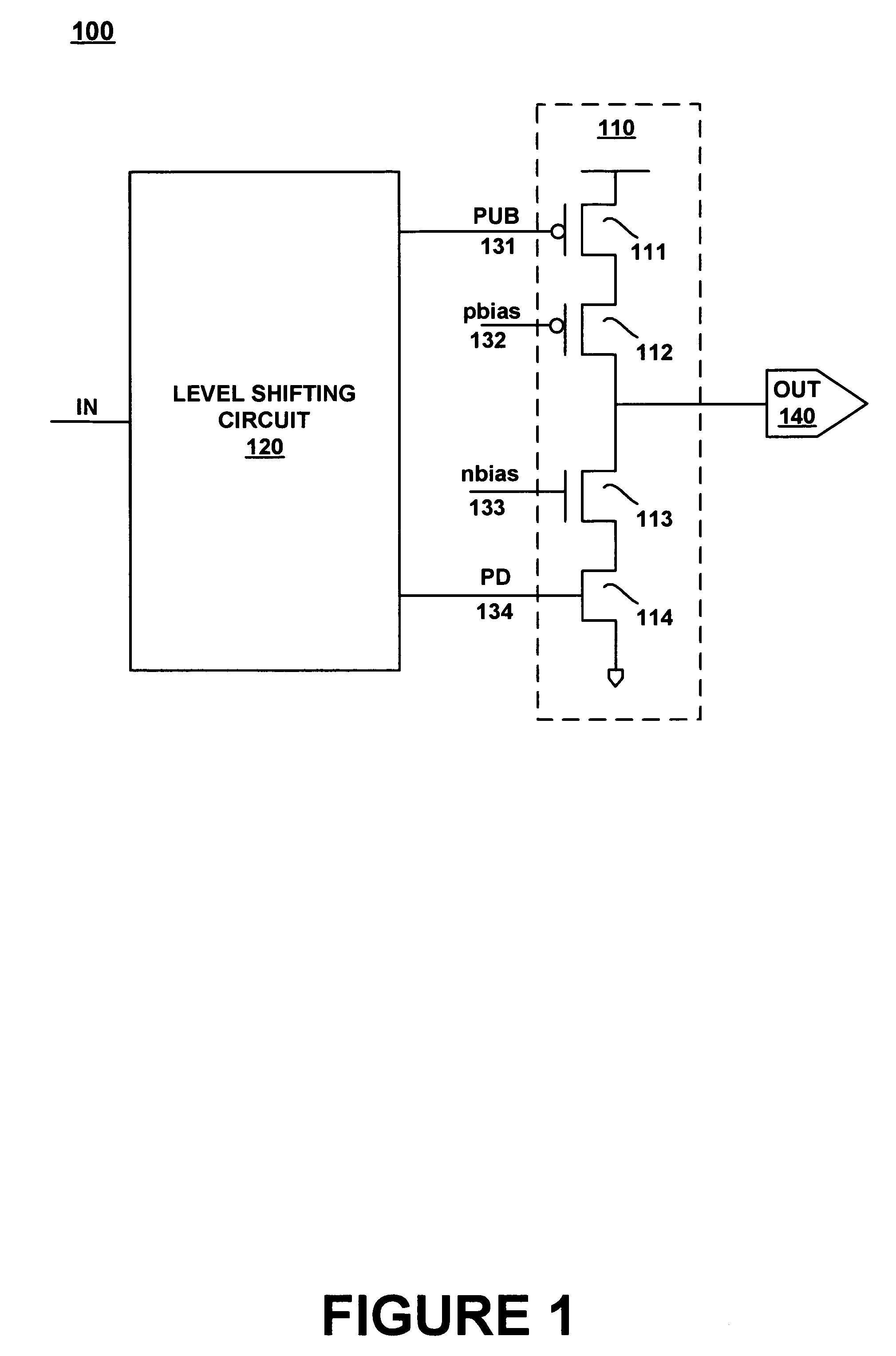
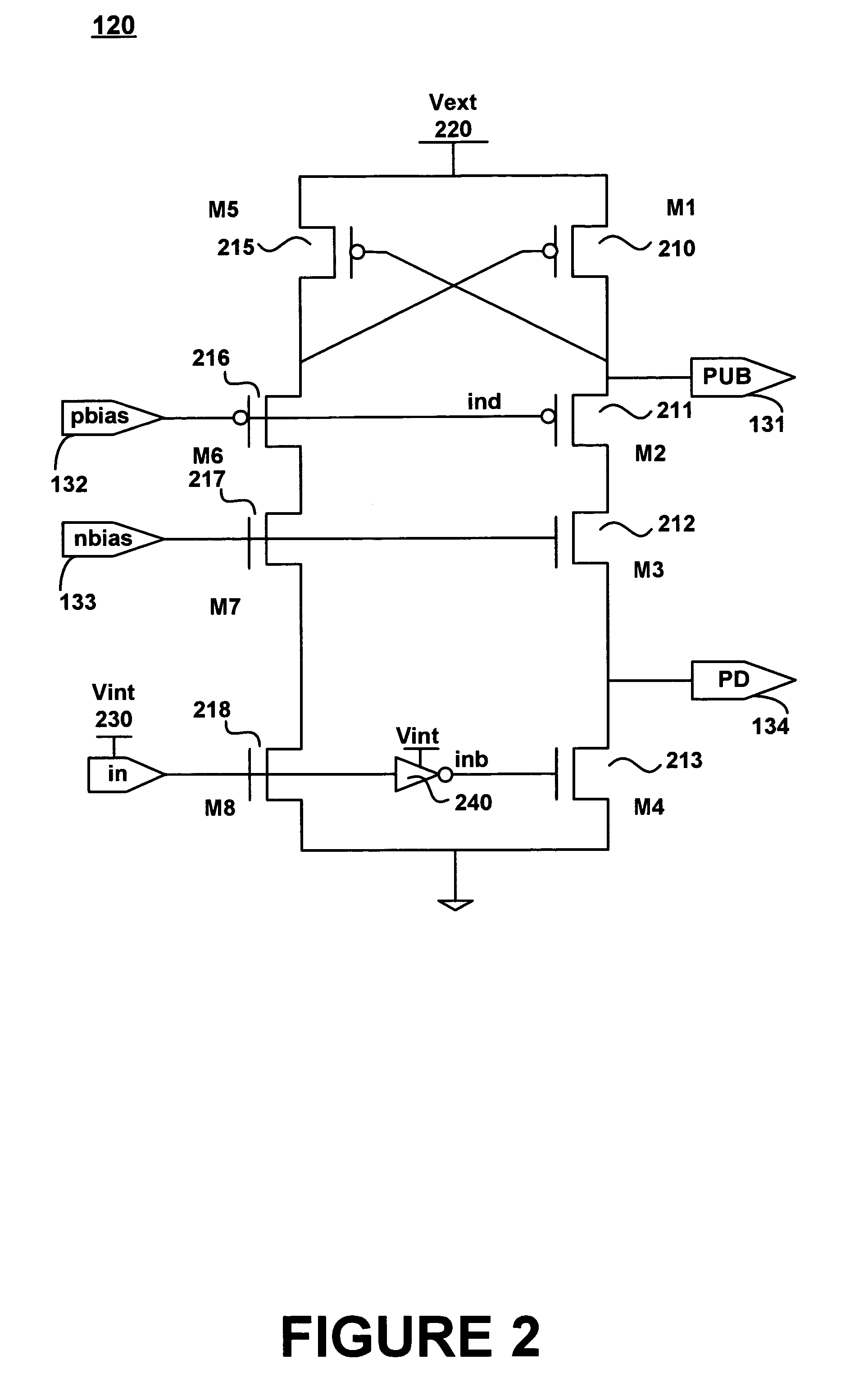
[0019]Reference will now be made in detail to embodiments of the present invention, examples of which are illustrated in the accompanying drawings. While the present invention will be described in conjunction with the following embodiments, it will be understood that they are not intended to limit the present invention to these embodiments alone. On the contrary, the present invention is intended to cover alternatives, modifications, and equivalents which may be included within the spirit and scope of the present invention as defined by the appended claims. Furthermore, in the following detailed description of the present invention, numerous specific details are set forth in order to provide a thorough understanding of the present invention. However, embodiments of the present invention may be practiced without these specific details. In other instances, well-known methods, procedures, components, and circuits have not been described in detail so as not to unnecessarily obscure aspe...


PUM


Abstract

Embodiments of the present invention recite a level shifting circuit for high voltage protection. In embodiments of the present invention, the level shifting circuit comprises a first transistor, a second transistor, a third transistor, and a fourth transistor coupled in a cascode configuration. The circuit further comprises a fifth transistor, a sixth transistor, a seventh transistor, and an eighth transistor coupled in a cascode configuration. The level shifting circuit further comprises an output coupled with the source of the first transistor, the gate of the seventh transistor, and with the drain of the second transistor. A first inverter is coupled with a second inverter in series and an input signal conveyed to the first inverter dynamically controls the bias level for said second and sixth transistors.

Description

RELATED APPLICATIONS[0001]The present application claims priority to USPTO provisional application No. 60 / 482,972 filed Jun. 26, 2003, entitled “Dynamic Biased Wide Swing Level Shifting Circuit for High Speed High Voltage Protection Input / Outputs,” by Tao Peng, assigned to the assignee of the present invention, and which is hereby incorporated by reference in its entirety herein.FIELD OF THE INVENTION[0002]The present invention relates generally to electronic circuits and in particular to output circuits.BACKGROUND OF THE INVENTION[0003]A integrated circuit (IC) process technology advances to higher densities, the feature size of a transistor is reduced enabling low-voltage high speed operation and high density layout. Another result of the reduced feature size is to also reduce the transistor's gate oxide voltage tolerance. Some conventional input / output (I / O) standards require an IC to interface with external voltages that are higher than the internal voltages used within the IC. ...

Claims


Application Information

Patent Timeline
Patent Type & Authority Patents(United States)
IPC IPC(8): H03K19/094
CPCH03K3/356113H03K19/018521H03K17/102
Inventor PENG, TAO
Owner GULA CONSULTING LLC
Why Eureka
Try Eureka