Grid driving circuit, array substrate, display device and driving method

A technology for a gate drive circuit and a display device, which is applied in the fields of gate drive circuits and array substrates, can solve the problems of high overall power consumption of the display device, and achieve the effects of ensuring display quality and reducing overall power consumption.

Active Publication Date: 2013-12-25
BEIJING BOE OPTOELECTRONCIS TECH CO LTD
View PDF6 Cites 37 Cited by
  • Summary
  • Abstract
  • Description
  • Claims
  • Application Information

AI Technical Summary

Problems solved by technology

[0005] Embodiments of the present invention provide a gate driving circuit, an array substrate including the gate driving circuit, a display device, and a driving method, which are used to solve the problem of large overall power consumption of the display device when the existing gate driving circuit is in operation. question

Method used


Image

  • Grid driving circuit, array substrate, display device and driving method
  • Grid driving circuit, array substrate, display device and driving method
  • Grid driving circuit, array substrate, display device and driving method

Examples


Embodiment 1

[0112] The driving method provided by the embodiment of the present invention will be described below in combination with the first embodiment.

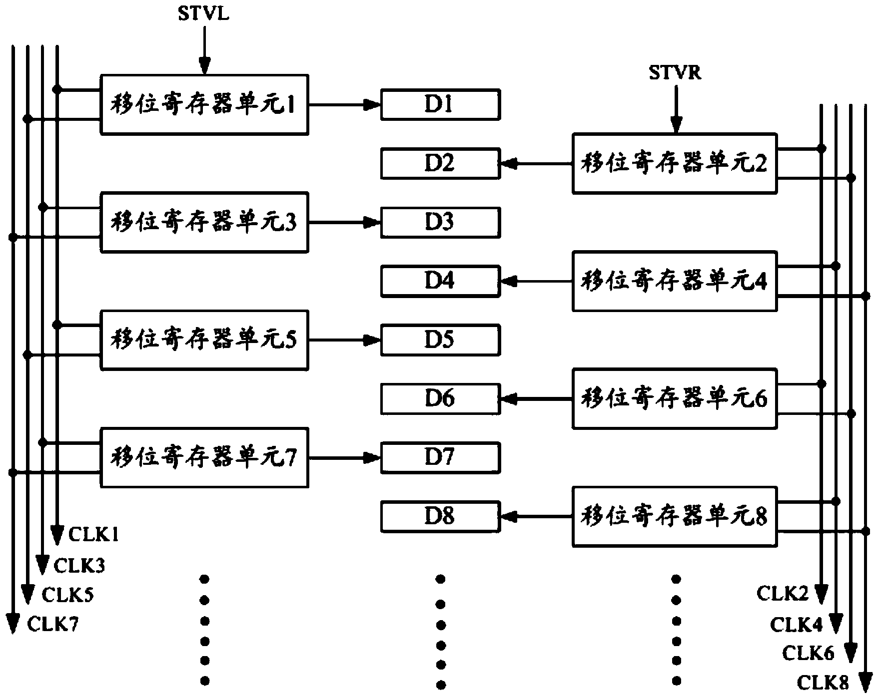
[0113] Embodiment 1, this embodiment is still based on figure 2 The structure diagram of the gate driving circuit shown is taken as an example to illustrate the first driving method, and other situations are similar, and will not be listed here.

[0114] Figure 4 Shown is the input timing diagram of the first sub-circuit of the gate driving circuit of this embodiment, and the input timing diagrams of other sub-circuits are similar, and will not be listed here. Figure 4 Including the frame start signal (STVL signal and STVR signal), where the high-level pulse of the STVL signal is output, and the high-level pulse of the CLK1 / CLK3 / CLK5 / CLK7 signal is output in sequence, so that the shift register 1 / 3 / 5 / 7 generates the gate scanning signal for driving the gate signal lines of the 1 / 3 / 5 / 7 row (that is, the gate scanning signal of t...

Embodiment 2

[0122] Embodiment two, this embodiment is still based on figure 2 The structure diagram of the gate driving circuit shown is taken as an example to illustrate the first driving method, and other situations are similar, and will not be listed here.

[0123] In this embodiment, on the basis of the first embodiment, the pixel pre-charging process is added. For the input timing diagram of the first sub-circuit of the gate drive circuit, refer to Figure 8 As shown, the input timing diagrams of other sub-circuits are similar to this, and will not be listed here. Figure 8The pulse duration of the high-level pulse of the STVL signal is still H1, and the pulse duration of the high-level pulse of the generated clock control signal CLK1 / CLK3 / CLK5 / CLK7 signal is H1+H2, and the high-level pulse of the STVR signal The pulse duration of the pulse is still H1, and the pulse duration of the high-level pulse of the generated CLK2 / CLK4 / CLK6 / CLK8 signal is H1+H2, that is, the adjacent two clo...


PUM


Abstract

The embodiment of the invention discloses a grid driving circuit, an array substrate, a display device and a driving method. The grid driving circuit is used for solving the problem that a large amount of power is consumed when an existing grid driving circuit works. The grid driving circuit comprises at least one sub-circuit, wherein each sub-circuit comprises M shifting register units, and M is a positive integer which is equal to or lager than 3; in any sub-circuit, the shifting register units used for driving odd grid signal lines are connected in sequence, the output end of an upper-level shifting register unit in the shifting register units used for driving the odd grid signal lines is connected with the input end of a lower-level shifting register unit, the shifting register units used for driving even grid signal lines are connected in sequence, and the output end of an upper-level shifting register unit in the shifting register units used for driving the even grid signal lines is connected with the input end of a lower-level shifting register unit. The grid driving circuit, the array substrate, the display device and the driving method have the advantages that power consumption is reduced on the premise that display quality is guaranteed.

Description

technical field [0001] The present invention relates to the field of display technology, in particular to a gate drive circuit and an array substrate including the gate drive circuit. Display device and driving method. Background technique [0002] In recent years, with the rapid development of display technology, Flat Panel Display (FPD) has the characteristics of complete planarization, light weight, thin thickness and power saving, which is in line with the development trend of future image display devices. Currently, common flat panel display devices include plasma display panel (Plasma DisplayPanel, PDP), liquid crystal display (Liquid Crystal Display, LCD), field emission display (Field Emission Display, FED), organic light-emitting diode (Organic Light-Emitting Diode, OLED) Display devices, projection display devices, etc. [0003] In the field of flat panel display, LCD is known as the flat panel display device with the fastest development, the most mature technolo...

Claims


Application Information

Patent Timeline
Patent Type & Authority Applications(China)
IPC IPC(8): G09G3/36G09G3/20
Inventor 徐帅王智勇朱红张郑欣
Owner BEIJING BOE OPTOELECTRONCIS TECH CO LTD
Why Eureka
Try Eureka