Thin film transistor array substrate, manufacturing method and display device

A thin-film transistor and array substrate technology, which is applied in the field of liquid crystal display manufacturing of thin-film transistors, can solve the problems of affecting the shading effect of the drain and reducing the display effect of the display device, so as to avoid the effect and ensure the display quality

Active Publication Date: 2015-03-25
TCL CHINA STAR OPTOELECTRONICS TECH CO LTD
View PDF5 Cites 19 Cited by
  • Summary
  • Abstract
  • Description
  • Claims
  • Application Information

AI Technical Summary

Problems solved by technology

[0004] However, the traditional COA black matrix is ​​usually located between the drain of the thin film transistor and the pixel electrode. In order to realize the electrical connection between the drain and the pixel electrode, it is necessary to form a via hole in the black matrix, which will affect the black matrix to the drain. The shading effect of the pole causes the drain to reflect the light from the side of the via hole, which reduces the display effect of the display device

Method used


Image

  • Thin film transistor array substrate, manufacturing method and display device
  • Thin film transistor array substrate, manufacturing method and display device
  • Thin film transistor array substrate, manufacturing method and display device

Examples


Embodiment Construction

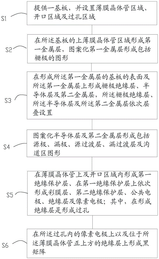
[0035] The following will clearly and completely describe the technical solutions in the embodiments of the present invention with reference to the accompanying drawings in the embodiments of the present invention. Obviously, the described embodiments are only some, not all, embodiments of the present invention. Based on the embodiments of the present invention, all other embodiments obtained by persons of ordinary skill in the art without making creative efforts belong to the protection scope of the present invention.

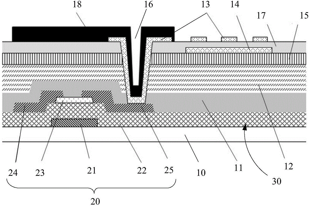
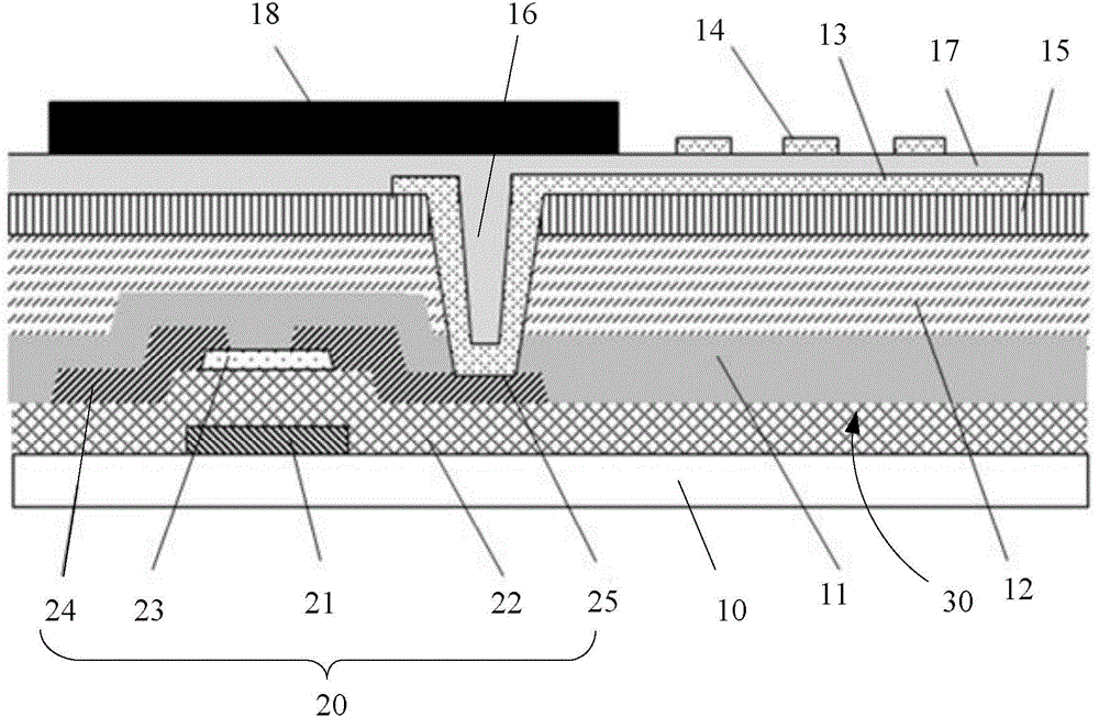
[0036] The invention protects a thin film transistor array substrate and a display device with the thin film transistor array substrate. The thin film transistor array substrate includes a substrate and a plurality of data lines and a plurality of gate lines intersecting on the substrate 1 (data lines and gate lines are not specifically shown in the figure), and the data lines and gate lines divide the substrate into grid lines. A plurality of thin film transi...


PUM


Abstract

The invention provides a thin film transistor array substrate. The thin film transistor array substrate comprises a substrate body, a plurality of thin film transistors and a plurality of opening areas, wherein the thin film transistors are formed on the substrate body and arrayed in a grid mode. The thin film transistor array substrate further comprises a first insulating protective layer, a color film layer, pixel electrodes, a common electrode, a second insulating protective layer, a via hole, an insulating layer and a black matrix, the first insulating protective layer is formed on the thin film transistors and the opening areas, each thin film transistor comprises a grid electrode and a drain electrode, the pixel electrodes are connected with the drain electrodes through the via hole, and the black matrix is located on the insulating layer or the pixel electrodes and the insulating layer and used for shielding the thin film transistors and the via hole. The invention further provides a display device and a manufacturing method of the thin film transistor array substrate.

Description

technical field [0001] The invention relates to the field of liquid crystal display manufacturing of thin film transistors, in particular to a thin film transistor array substrate, a manufacturing method of the thin film transistor array substrate and a display device with the thin film transistor array substrate. Background technique [0002] With the advancement of science and technology, liquid crystal display devices are developing towards high transmittance, high resolution, low power consumption and other directions. Among them, the higher the resolution, the smaller the size of each color filter layer. When the side length of the color filter layer changes from tens of microns to more than ten microns, obviously, the size of the color filter layer has been greatly reduced. , at this time, if the width of the black matrix dividing the color filter layer remains unchanged, the black matrix will become obvious relative to the color filter layer, which will affect the dis...

Claims


Application Information

Patent Timeline
Patent Type & Authority Applications(China)
IPC IPC(8): G02F1/1362G02F1/1368H01L27/12H01L21/77
CPCG02F1/136209G02F1/136286G02F1/1368G02F1/136295H01L27/1214H01L27/1259G02F1/1362H01L21/77H01L27/12
Inventor 徐向阳
Owner TCL CHINA STAR OPTOELECTRONICS TECH CO LTD
Why Eureka
Try Eureka