

Package substrate with improved reliability
- Summary
- Abstract
- Description
- Claims
- Application Information
AI Technical Summary
Benefits of technology
Problems solved by technology
Method used
Image

Examples
Embodiment Construction
[0014]The following sets forth a detailed description of various embodiments intended to be illustrative of the invention and should not be taken to be limiting.
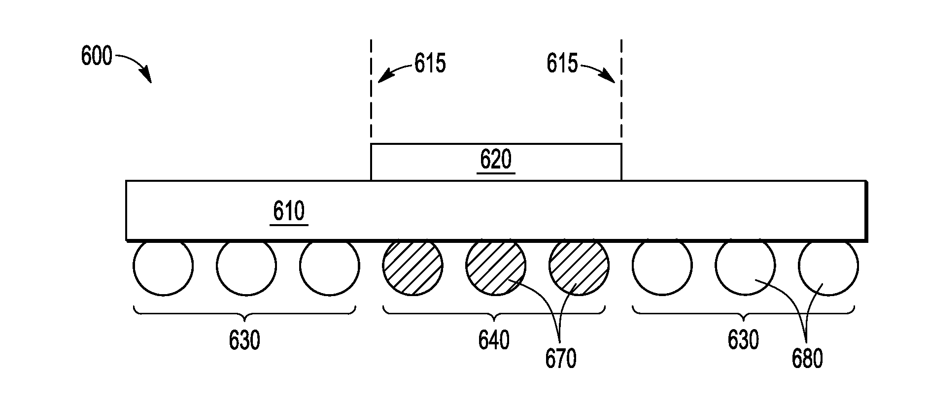
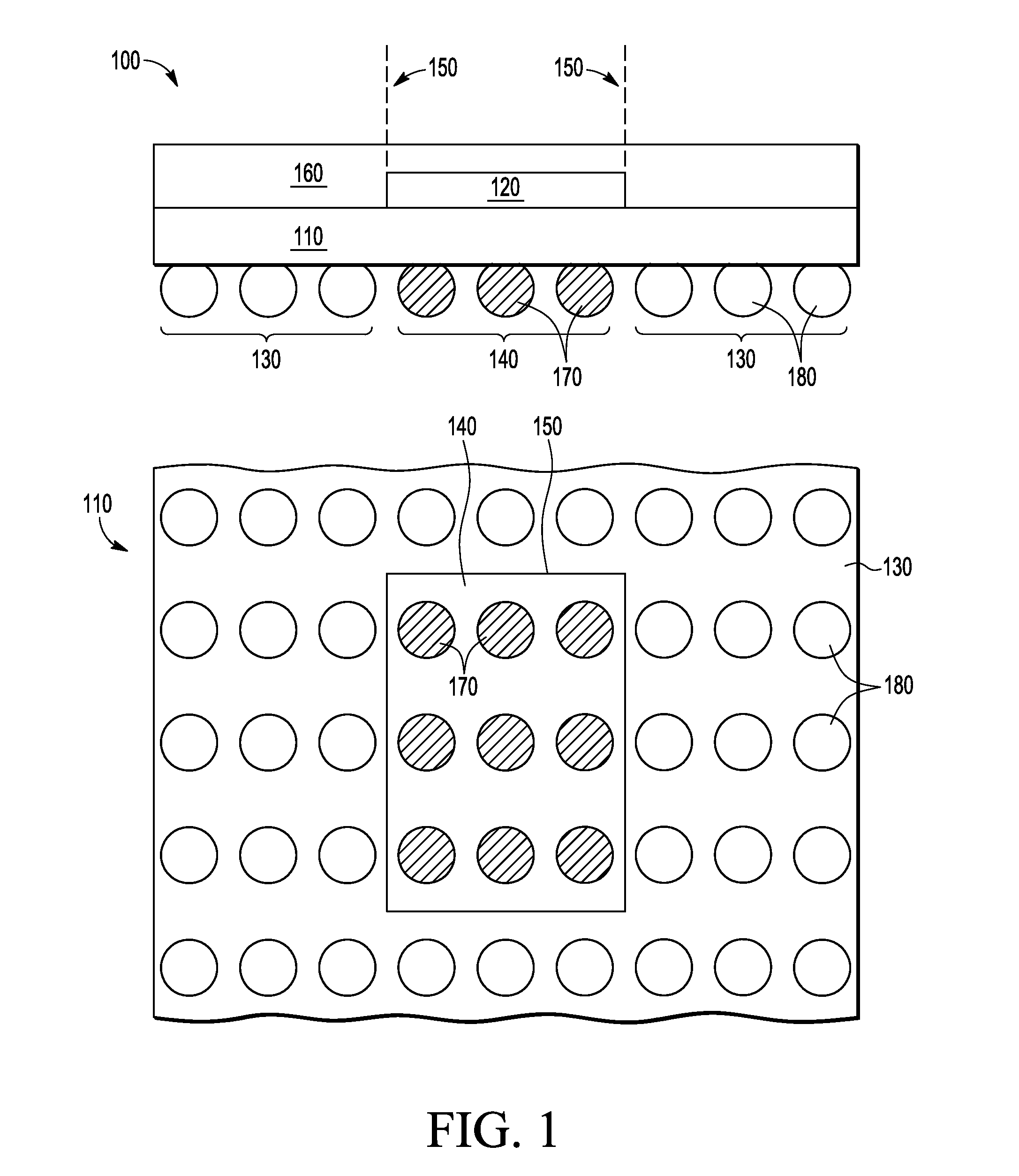
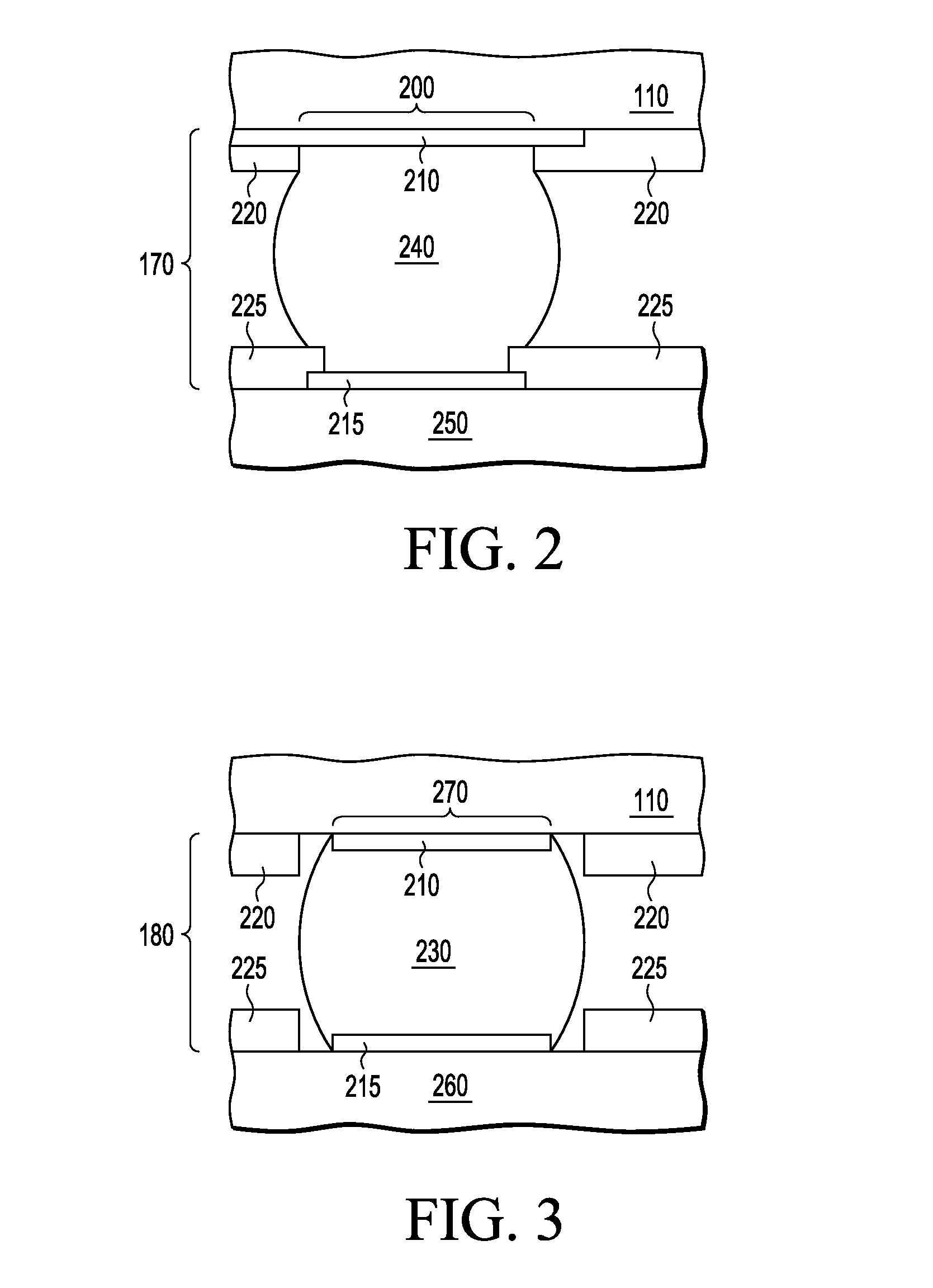
[0015]Due to increasingly stringent reliability criteria expected of packaged semiconductor devices, it is generally desirable to increase the reliability and lifespan of solder connections used in such devices. The present disclosure provides for improving reliability and lifespan of solder connections by using solder mask defined (SMD) pads in a region on a bottom surface of a package substrate that is under a die attached to a top surface (which is opposite the bottom surface) of the package substrate, and non-solder mask defined (NSMD) pads in another region that is not under the die, as described herein. The selected placement of SMD pads and NSMD pads on the package substrate relative to the die results in solder connections that are better able to withstand the different thermal and mechanical forces experienced in th...
PUM
 Abstract
Description
Claims
Application Information