Substrate structure

a substrate and structure technology, applied in the field of substrate structure, can solve problems such as fatal short circuits, and achieve the effect of increasing the bonding between solder balls

Inactive Publication Date: 2009-05-07
ADVANCED SEMICON ENG INC
View PDF6 Cites 72 Cited by
  • Summary
  • Abstract
  • Description
  • Claims
  • Application Information

AI Technical Summary

Benefits of technology

[0008]It is an object of the present invention to provide a substrate structure, wherein the openings of the solder mask on the substrate to expose the solder pa

Problems solved by technology

However, when the exposed portions of the solder pads 110 are increased, the adjacent solder balls 130 are l

Method used


Image

  • Substrate structure
  • Substrate structure
  • Substrate structure

Examples


Embodiment Construction

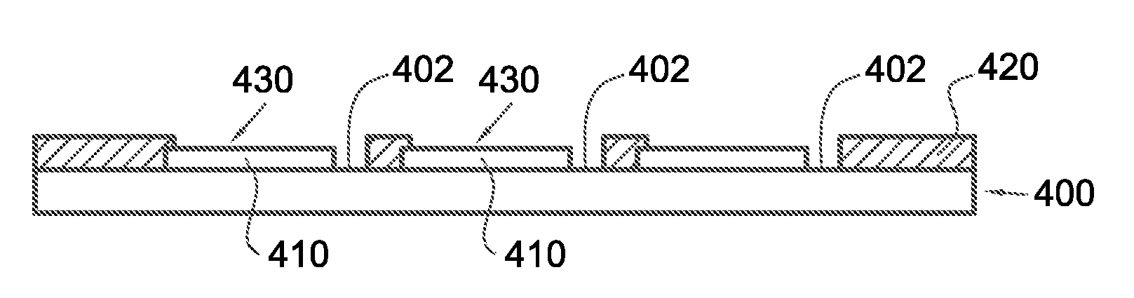
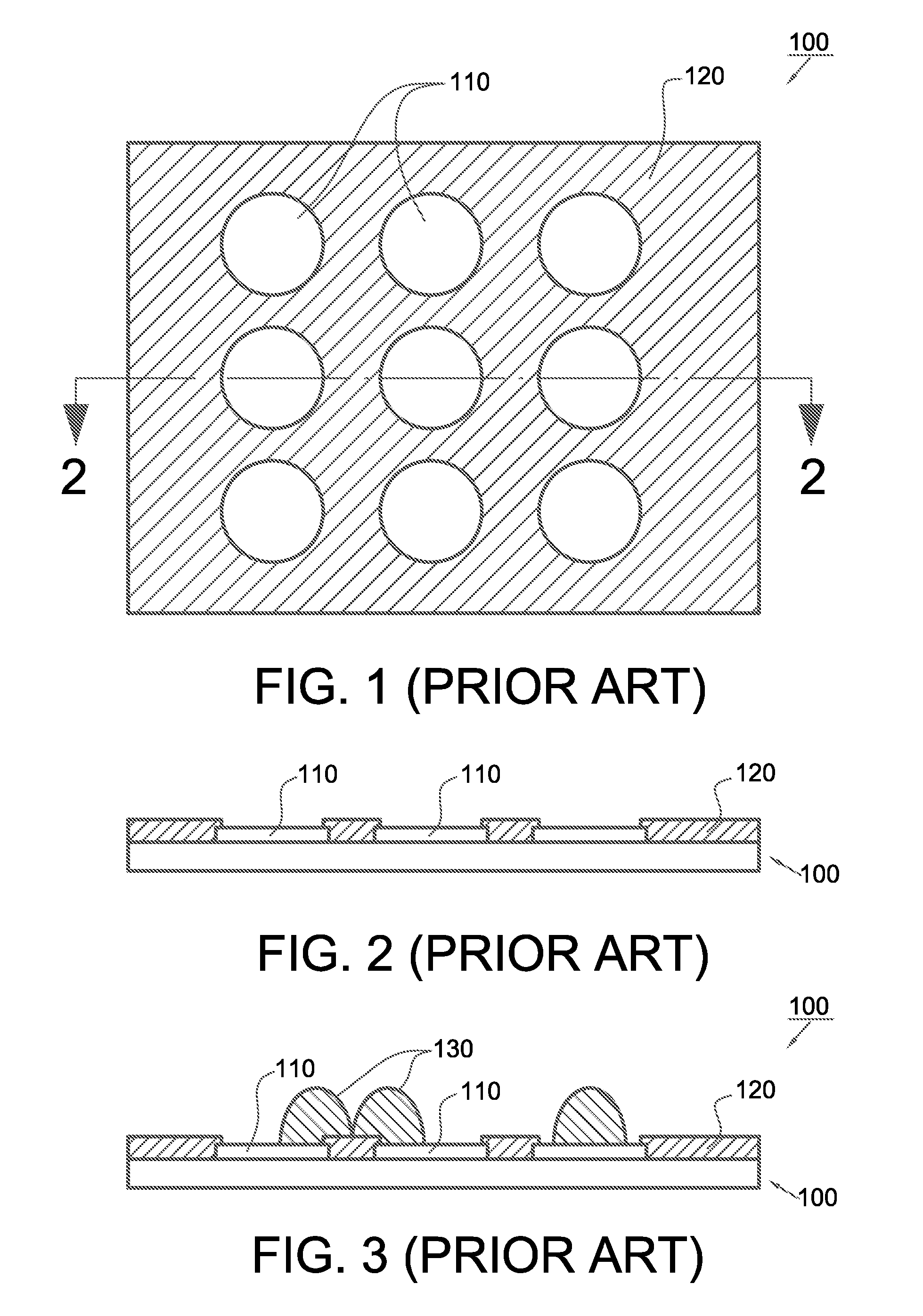
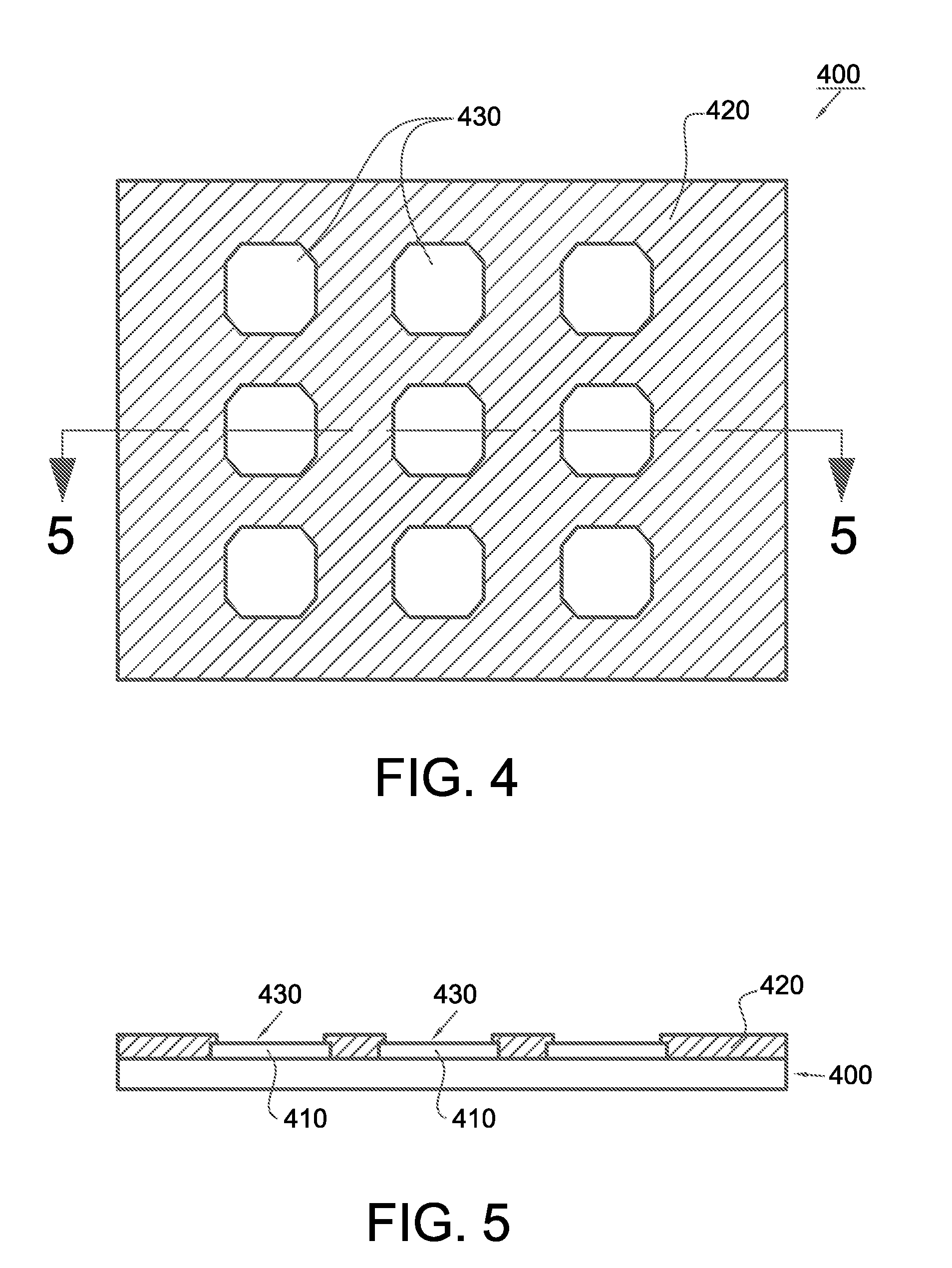
[0023]Referring to FIGS. 4 and 5, the substrate structure 400 of the present invention is provided with a plurality of solder pads 410 thereon arranged in the shape of a matrix. A solder mask 420 covers the substrate 400 and has a plurality of openings 430 to respectively expose the portions of the solder pads 410, wherein the openings 430 have the shape of a polygon of at least five sides, such as an octagon. Besides, referring to FIGS. 6 and 7, the openings 430 can also be a ten-sided polygon or dodecagon.

[0024]To better illustrate the advantage of the present invention, FIG. 8 shows two openings with the shape of a circle 440 to expose the corresponding solder pads in the art and two openings with the shape of a polygon 450 to expose the corresponding solder pads according to the present invention. The polygons 450 are arranged in such a manner that the nearest sides 452 of the two polygons 450 are parallel to each other. As can be seen from the figure, the shortest distance betw...


PUM


Abstract

A substrate structure is provided. A plurality of solder pads is positioned on a substrate. A solder mask covers the substrate and has a plurality of openings to respectively expose portions of the solder pads, wherein the openings have the shape of a polygon of at least five sides.

Description

CROSS REFERENCE TO RELATED APPLICATION[0001]This application claims the priority benefit of Taiwan Patent Application Serial Number 096141979 filed Nov. 7, 2007, the full disclosure of which is incorporated herein by reference.BACKGROUND OF THE INVENTION[0002]1. Field of the Invention[0003]The invention relates to a substrate structure and more particularly, to a substrate structure that the openings of the solder mask on the substrate have special shape.[0004]2. Description of the Related Art[0005]Miniaturization of semiconductor device size has been an important topic in the art when the device requires more I / O pins along with the increase of device density. Relatively, the ball grid array (BGA) package is an efficient packaging technology since it can provide more I / O pins.[0006]Referring to FIGS. 1 and 2, the conventional BGA substrate 100 is provided with a plurality of solder pads 110 thereon arranged in the shape of a matrix. A solder mask 120 covers the substrate 100 and ha...

Claims


Application Information

Patent Timeline
IPC IPC(8): H01R12/04
CPCH01L23/49811H01L23/49838H05K3/3436H05K3/3452H05K2201/099H01L2924/0002H05K2201/10734H01L2924/00
Inventor CHEN, CHIA CHINGDING, YI CHUAN
Owner ADVANCED SEMICON ENG INC
Why Eureka
Try Eureka