Manufacturing method of semiconductor device

a manufacturing method and semiconductor technology, applied in semiconductor devices, semiconductor/solid-state device details, electrical equipment, etc., can solve the problems of warping in the semiconductor wafer, poor printing alignment accuracy, and increased accuracy of alignment to form a conductive terminal in the subsequent screen printing process, so as to improve yield and reliability of a bga-type semiconductor device. , the effect of preventing warping

Active Publication Date: 2006-09-05
SEMICON COMPONENTS IND LLC
View PDF9 Cites 59 Cited by
  • Summary
  • Abstract
  • Description
  • Claims
  • Application Information

AI Technical Summary

Benefits of technology

[0016]A semiconductor wafer is prevented from warping by forming a film of cushioning material, a protection film or a photoresist film to provide an opening in the protection film by spray coating to mak

Problems solved by technology

There arises a problem that the larger shrinking in the bottom of the V-shaped groove VG causes a warping in the semiconductor wafer.
The warping in the semiconductor wafer poses a problem to a manufacturing process that follows.
Especially in a process s

Method used


Image

  • Manufacturing method of semiconductor device
  • Manufacturing method of semiconductor device
  • Manufacturing method of semiconductor device

Examples


Embodiment Construction

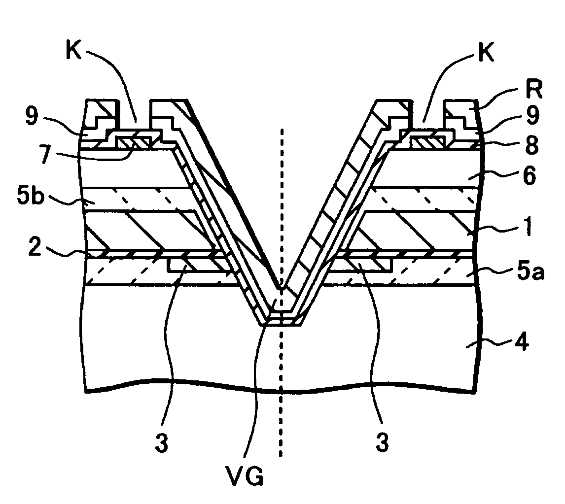
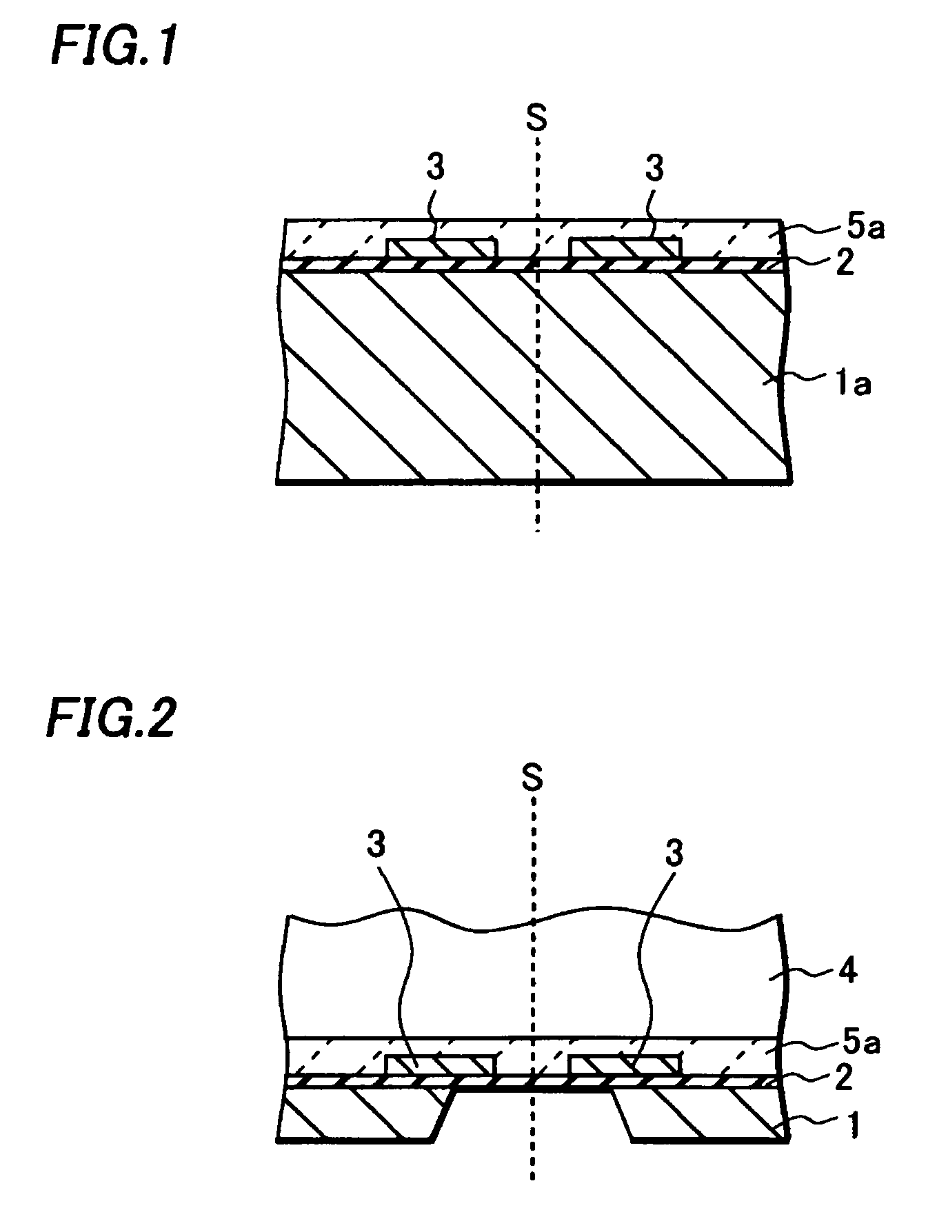
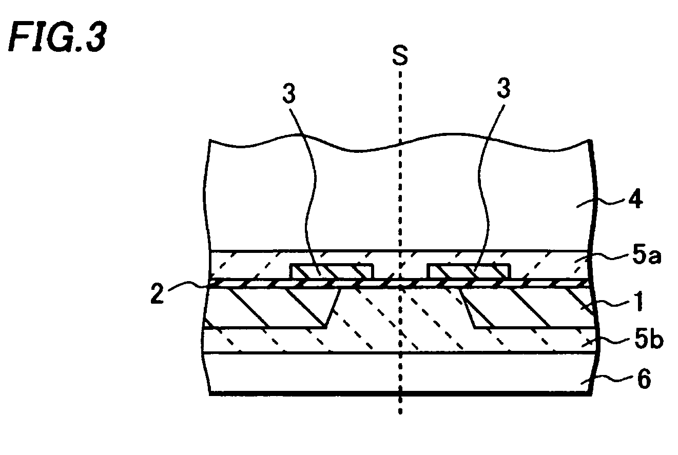
[0030]A manufacturing method of a semiconductor device according to an embodiment of this invention will be explained referring to figures hereinafter. FIGS. 1–6 are cross-sectional views showing the manufacturing method of the semiconductor device according the embodiment of this invention.

[0031]First, a semiconductor wafer 1a having a plurality of semiconductor dice 1 is provided, as shown in FIG. 1. The semiconductor dice 1 are CCD image sensors, for example, and are manufactured by semiconductor wafer processing. A pair of first wirings 3 made mainly of aluminum or copper are formed to be 1 μm thick by sputtering on a insulation film 2 formed on the semiconductor wafer 1a.

[0032]Each of the pair of first wirings 3 is formed facing each other across a border line (called a dicing line or a scribe line) S to divide the semiconductor wafer into individual dice. Or, a first wiring 3 may be formed extending across the border line S and divided into a pair of first wirings 3 later on....


PUM


Abstract

A first glass substrate is bonded through a resin to a top surface of a semiconductor wafer on which a first wiring is formed. A second glass substrate is bonded to a back surface of the semiconductor wafer through a resin. A V-shaped groove is formed by notching from a surface of the second glass substrate through a part of the first glass substrate. A second wiring connected with the first wiring and extending to the surface of the second glass substrate is formed. A protection film composed of an organic resin and a photoresist layer to provide the protection film with an opening are formed on the second wiring by spray coating. A conductive terminal is formed by screen printing using the protection film as a solder mask. A cushioning material may be formed on the second glass substrate by spray coating.

Description

BACKGROUND OF THE INVENTION[0001]1. Field of the Invention[0002]This invention relates to a manufacturing method of a BGA (Ball Grid Array) type semiconductor device which has ball-shaped conductive terminals.[0003]2. Description of the Related Art[0004]A CSP (Chip Size Package) receives attention in recent years as a three-dimensional mounting technology as well as a new packaging technology. The CSP means a small package having about the same outside dimensions as those of a semiconductor die packaged in it.[0005]The BGA type semiconductor device has been known as a kind of CSP. A plurality of ball-shaped conductive terminals made of metal such as solder is arrayed in a grid pattern on one principal surface of a package of the BGA type semiconductor device and is electrically connected with the semiconductor die mounted on the other side of the package.[0006]When the BGA type semiconductor device is mounted into electronic equipment, the semiconductor die and external circuit on a...

Claims


Application Information

Patent Timeline
IPC IPC(8): H01L21/44H01L21/68H01L21/768H01L23/31H01L23/48H01L23/485
CPCH01L21/6835H01L23/3114H01L23/3185H01L23/481H01L21/76898H01L2924/1305H01L24/10H01L2221/6834H01L2221/68377H01L2224/16H01L2924/01057H01L2924/01078H01L2924/01079H01L2924/01019H01L2924/00H01L2224/05008H01L2224/05001H01L2224/05569H01L2224/05548H01L2224/02377H01L24/05H01L2224/05644H01L2924/00014H01L2224/05655H01L2224/05124H01L2224/05147
Inventor NOMA, TAKASHISHINOGI, HIROYUKISUZUKISEKI, YOSHINORIKUHARA, KOICHITAKAO, YUKIHIROYAMADA, HIROSHI
Owner SEMICON COMPONENTS IND LLC
Why Eureka
Try Eureka