Semiconductor device and manufacturing method of the same

a technology of semiconductors and manufacturing methods, applied in the direction of basic electric elements, hand carts, transportation and packaging, etc., can solve problems such as degrading work efficiency

Active Publication Date: 2005-09-08
SANYO ELECTRIC CO LTD
View PDF16 Cites 60 Cited by
  • Summary
  • Abstract
  • Description
  • Claims
  • Application Information

AI Technical Summary

Problems solved by technology

Also there is a problem in step coverage of the second wiring 110.
Since the members having different thermal expansion coefficients are thus bond...

Method used


Image

  • Semiconductor device and manufacturing method of the same
  • Semiconductor device and manufacturing method of the same
  • Semiconductor device and manufacturing method of the same

Examples


Embodiment Construction

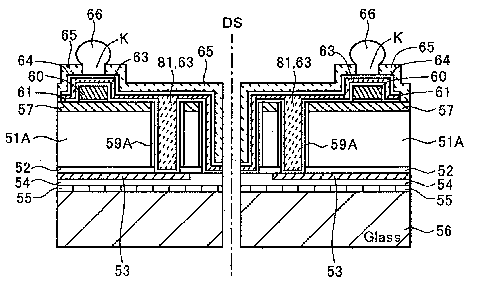
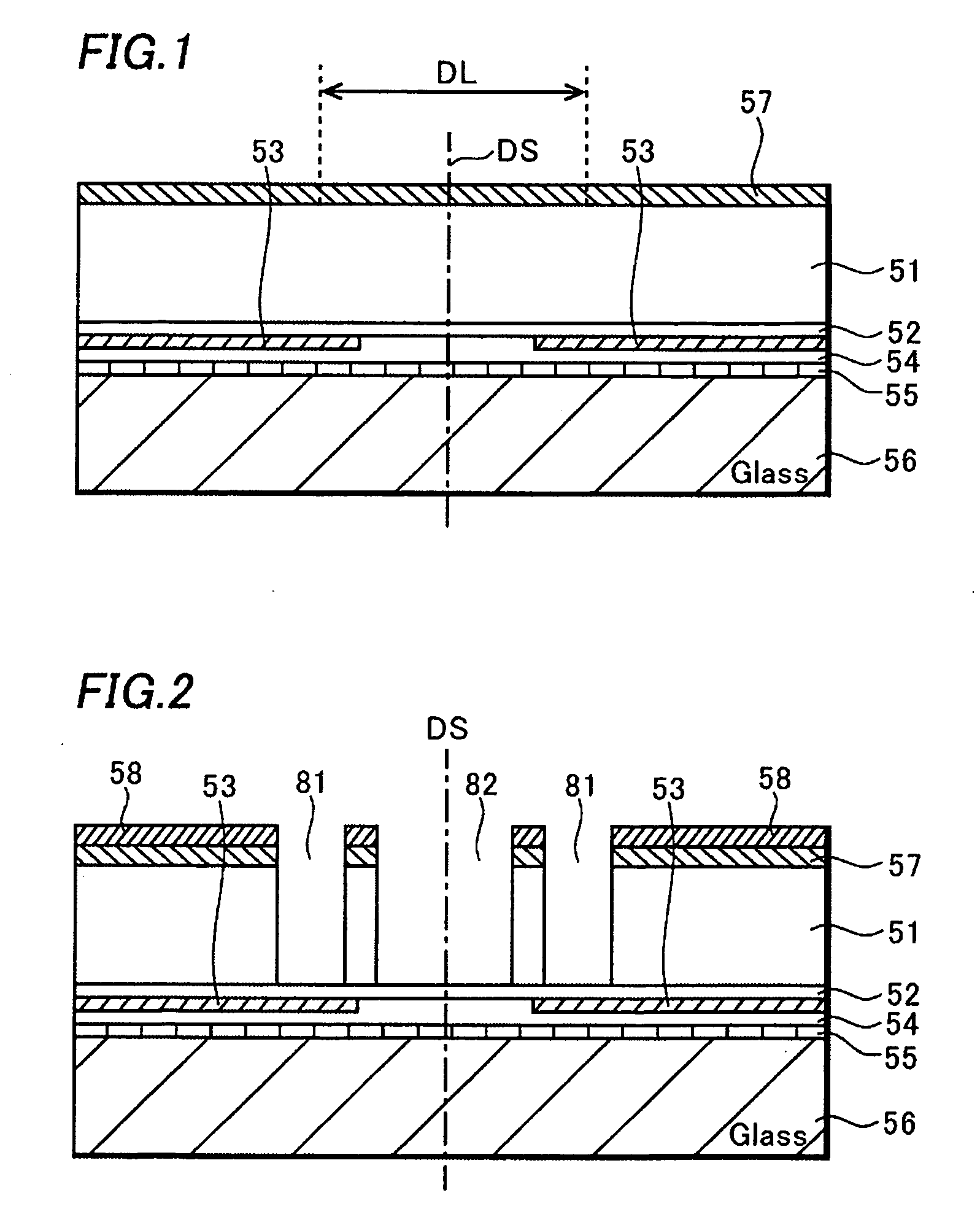
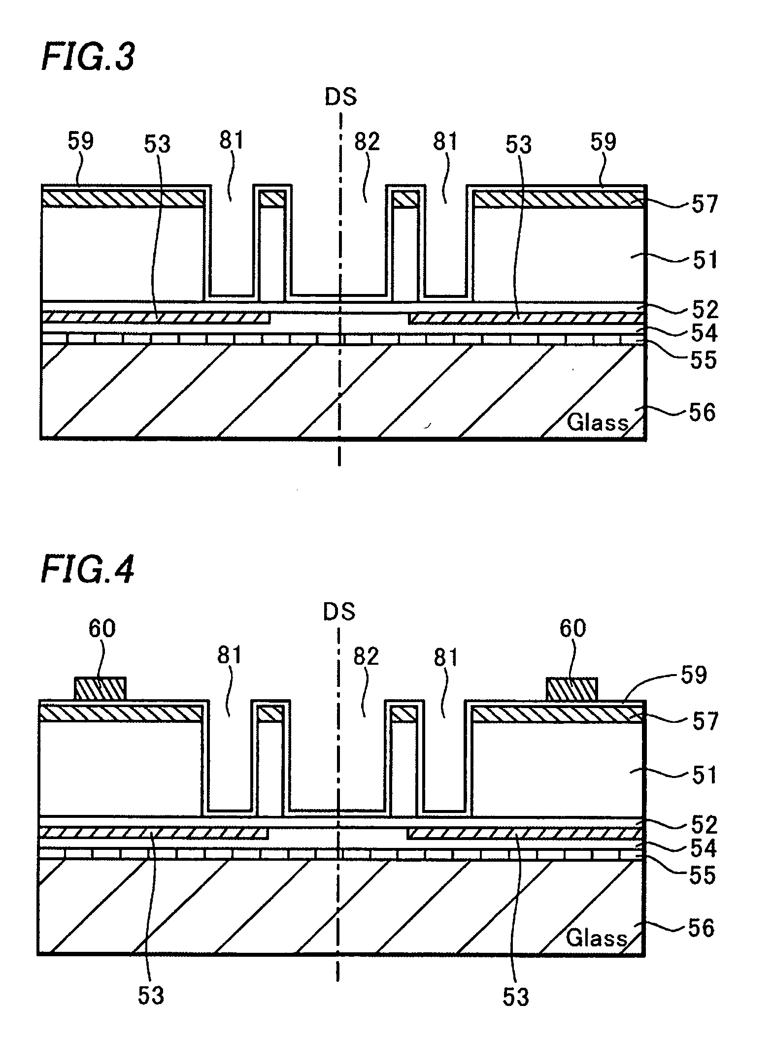
[0033] An embodiment of this invention will be described in detail, referring to figures hereinafter. First, a structure of the semiconductor device will be described. FIG. 11 is a cross-sectional view of the semiconductor device separated into individual dice by dicing a silicon wafer 51 along a center DS of a dicing line in a dicing line region DL after process steps to be described hereinafter.

[0034] A silicon die 51A as a semiconductor die is a CCD (Charge Coupled Device) image sensor chip, for example. A pad electrode 53 is formed on a top surface of the silicon die 51A through an interlayer insulation film 52 such as a BPSG (Boro-Phospho Silicate Glass) film. The pad electrode 53 is formed by extending a normal pad electrode used for wire bonding to the dicing line region DL (see FIG. 1) in and is also called an extended pad electrode.

[0035] The pad electrode 53 is covered with a passivation film 54 made of a silicon nitride film, for example. A glass substrate 56 is bonded ...


PUM


Abstract

This invention improves reliability of a semiconductor device and a manufacturing method thereof. A glass substrate is bonded on a surface of a silicon wafer formed with pad electrodes. Next, via holes are formed from a back surface of the silicon wafer to pad electrodes, and a groove is formed extending along a center line of a dicing line and penetrating the silicon wafer from its back surface. After then, in processes including heating treatment, cushioning pads, wirings, a solder mask, and solder balls are formed on the back surface of the silicon wafer. Finally, the silicon wafer bolstered by the glass substrate is separated into individual silicon dice by dicing.

Description

CROSS-REFERENCE OF THE INVENTION [0001] This invention is based on Japanese Patent Application No. 2004-40408, the content of which is incorporated by reference in its entirety. BACKGROUND OF THE INVENTION [0002] 1. Field of the Invention [0003] This invention relates to a semiconductor device of a chip size package type and a manufacturing method thereof. [0004] 2. Description of the Related Art [0005] CSP (Chip Size Package) has received attention in recent years as a three-dimensional mounting technology as well as a new packaging technology. The CSP means a small package having almost the same outside dimensions as those of a semiconductor die packaged in it. [0006] Conventionally, BGA (ball grip array) type semiconductor devices have been known as a kind of CSP. In this BGA type semiconductor device, a plurality of ball-shaped conductive terminals made of metal such as solder is arrayed in a grid pattern on one surface of the package, and electrically connected with the semicon...

Claims


Application Information

Patent Timeline
IPC IPC(8): H01L21/02H01L23/52H01L21/3205H01L21/768H01L21/84H01L23/02H01L23/12H01L23/31H01L23/48H01L23/485H01L23/522
CPCH01L21/76898H01L23/3114H01L24/13H01L2924/10253H01L2924/014H01L23/481H01L24/10H01L27/14636H01L27/1469H01L2224/13099H01L2224/16H01L2924/01013H01L2924/01022H01L2924/01029H01L2924/01032H01L2924/01033H01L2924/01073H01L2924/01074H01L2924/01075H01L2924/01078H01L2924/01079H01L2924/01082H01L2924/04941H01L2924/04953H01L2924/10329H01L2924/14H01L2924/01005H01L2924/01006H01L2924/01019H01L2924/01072H01L2924/00H01L2224/13H01L2224/05024H01L2224/05009H01L2224/05022H01L2224/05548H01L2224/05001H01L2224/05124H01L2224/05147H01L2224/05624H01L2224/05644H01L2224/05655H01L24/03H01L24/05H01L2924/0001H01L2224/02372H01L2224/0231H01L2224/13024H01L24/02H01L2924/00014H01L2224/02B62B3/108
Inventor KAMEYAMA, KOUJIROSUZUKIOKAYAMA, YOSHIO
Owner SANYO ELECTRIC CO LTD
Why Eureka
Try Eureka