Semiconductor chip bump connection apparatus and method

a technology of semiconductor chips and bumps, applied in the field of semiconductor chip bump connection apparatus and method, can solve problems such as adding to the overall cos

Active Publication Date: 2010-03-02
ATI TECH INC
View PDF9 Cites 67 Cited by
  • Summary
  • Abstract
  • Description
  • Claims
  • Application Information

AI Technical Summary

Problems solved by technology

However, the materials, tools and processing time required to form an array of pre-solders do represent cost items that add to the overall cost of producing a packaged semiconductor chip.

Method used


Image

  • Semiconductor chip bump connection apparatus and method
  • Semiconductor chip bump connection apparatus and method
  • Semiconductor chip bump connection apparatus and method

Examples


Embodiment Construction

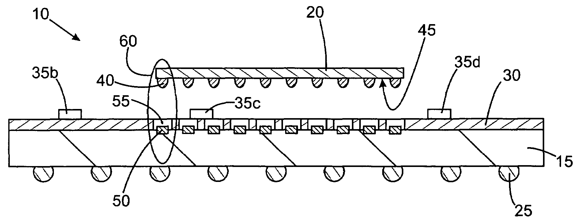
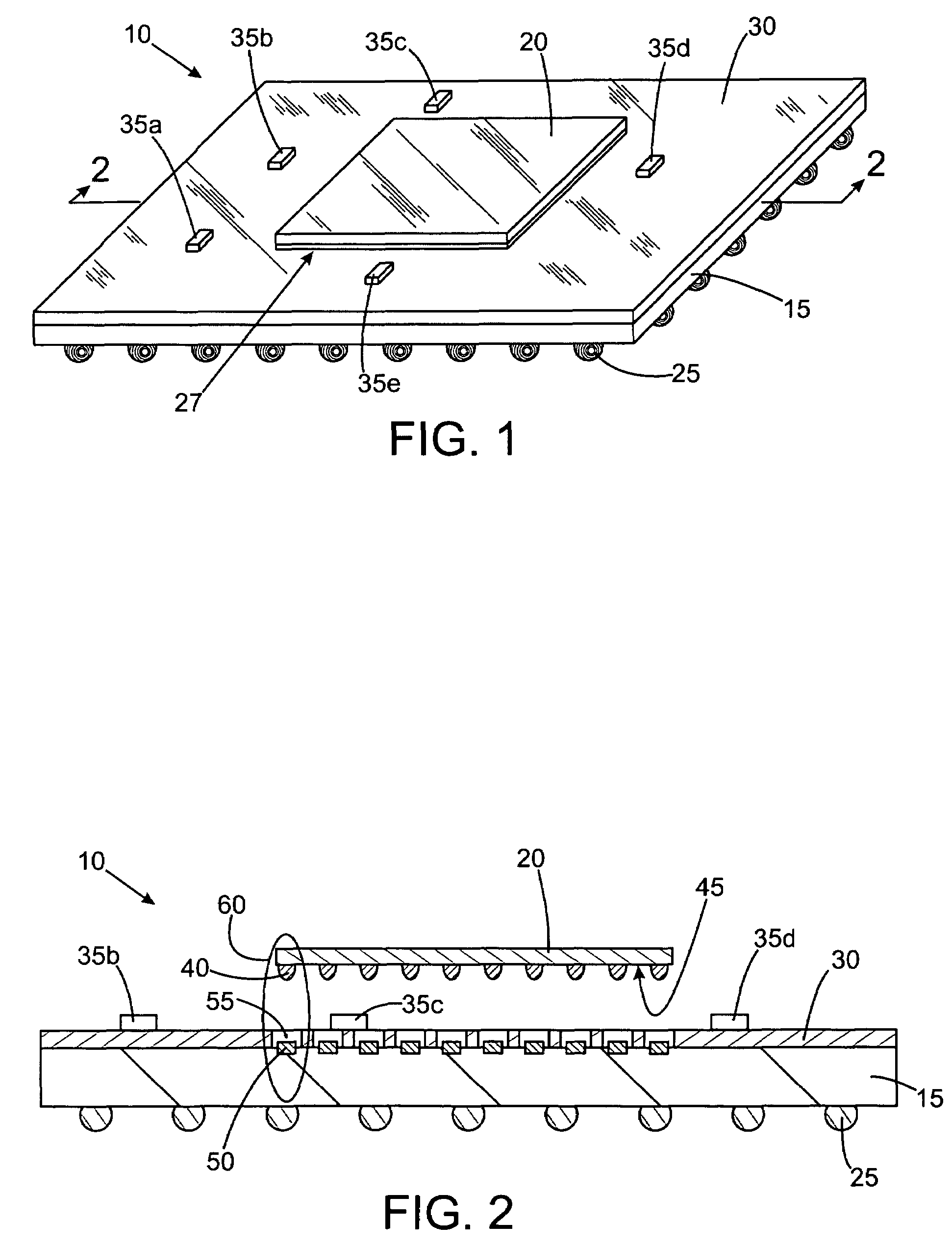
[0023]In the drawings described below, reference numerals are generally repeated where identical elements appear in more than one figure. Turning now to the drawings, and in particular to FIG. 1, therein is shown a pictorial view of an exemplary embodiment of a semiconductor chip package 10 that includes a substrate 15 adapted to receive a semiconductor chip or die 20 or multiple chips if desired. The chip 20 is flip-chip mounted to the substrate 15 and electrically connected thereto by way of a plurality of solder bumps which are not visible in FIG. 1, but will be in subsequent figures. The chip 20 may be any of a myriad of different types of circuit devices used in electronics, such as, for example, microprocessors, graphics processors, combined microprocessor / graphics processors, application specific integrated circuits, memory devices or the like, and may be single or multi-core or even stacked with additional dice. The package 10 may be lidless as depicted or fitted with any ty...


PUM


Abstract

Various semiconductor chip packages and methods of making the same are disclosed. In one aspect, a method of manufacturing is provided that includes coupling a solder bump to a side of a semiconductor chip and bringing the solder bump into contact with a conductor pad coupled to a substrate and positioned in an opening of a solder mask on the substrate. The conductor pad has a first lateral dimension and the opening has a second lateral dimension that is larger than the first lateral dimension. A metallurgical bond is established between the solder bump and the conductor pad.

Description

BACKGROUND OF THE INVENTION[0001]1. Field of the Invention[0002]This invention relates generally to semiconductor processing, and more particularly to methods and apparatus for electrically connecting a semiconductor chip to a package substrate.[0003]2. Description of the Related Art[0004]Many present day semiconductor chips are mounted to a package substrate that is, in-turn, mounted to another printed circuit board. A package substrate is typically larger in size than its companion chip. A package substrate serves several purposes. In one aspect, a package substrate provides a convenient interface between a typically small semiconductor chip and a normally much larger printed circuit board. In another aspect, a package substrate provides a mounting surface and conductive pathways for a variety of passive components, such as capacitors, that are useful for the operation of but cannot be easily incorporated into a semiconductor chip.[0005]In order to serve as an interface between a ...

Claims


Application Information

Patent Timeline
Patent Type & Authority Patents(United States)
IPC IPC(8): H01L21/44
CPCH01L23/49811H01L23/49816H01L24/16H01L24/81H05K3/3452H01L23/50H01L2224/13099H01L2224/13111H01L2224/16H01L2224/81136H01L2224/81801H01L2924/01027H01L2924/01029H01L2924/01046H01L2924/01049H01L2924/01051H01L2924/01078H01L2924/01079H01L2924/01082H01L2924/01322H01L2924/14H01L2924/19041H01L2924/19042H01L2924/19105H05K2201/0989H05K2201/10674H01L2924/01006H01L2924/01033H01L2924/01047H01L2924/0105H01L2224/16237H01L2224/05571H01L2224/05573H01L2224/05639H01L2224/05644H01L2224/05664H01L2224/05669H01L24/05H01L2924/00014
Inventor TOPACIO, RODEN R.CHAN, VINCENTYEUNG, FAN
Owner ATI TECH INC
Why Eureka
Try Eureka