Semiconductor device and manufacturing method of the same

a technology of semiconductor devices and penetrating electrodes, which is applied in the direction of semiconductor devices, semiconductor/solid-state device details, electrical apparatus, etc., can solve the problems of decreasing the reliability and yield and the reliability of the semiconductor device having the penetrating electrodes

Active Publication Date: 2006-04-27
SEMICON COMPONENTS IND LLC
View PDF43 Cites 74 Cited by
  • Summary
  • Abstract
  • Description
  • Claims
  • Application Information

AI Technical Summary

Benefits of technology

[0016] The invention provides a semiconductor device that includes a semiconductor die, a pad electrode disposed on the front surface of the semiconductor die, a refractory metal layer disposed on the pad electrode and having a melting point higher than a melting point of the pad electrode, a first protection layer disposed on the fro

Problems solved by technology

That is, the deformation of the pad electrode 52 causes a problem of decreasing the reliability of the semiconductor device having th

Method used


Image

  • Semiconductor device and manufacturing method of the same
  • Semiconductor device and manufacturing method of the same
  • Semiconductor device and manufacturing method of the same

Examples


Embodiment Construction

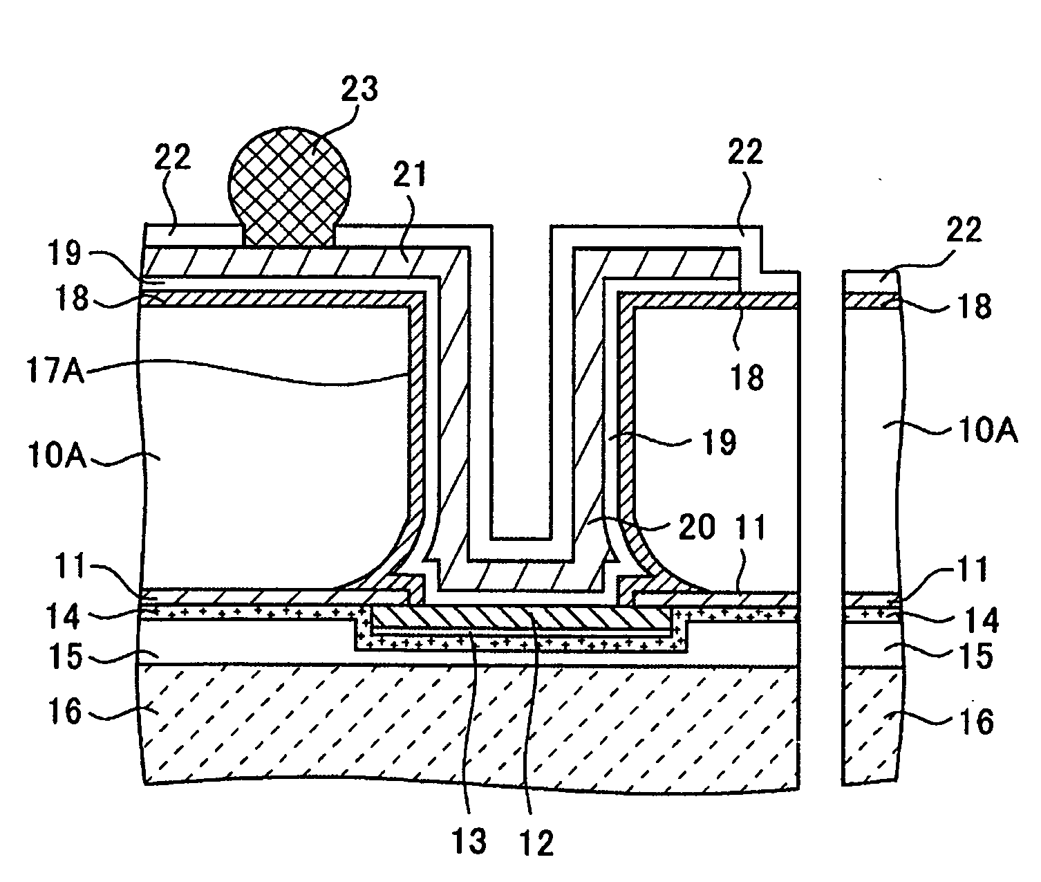
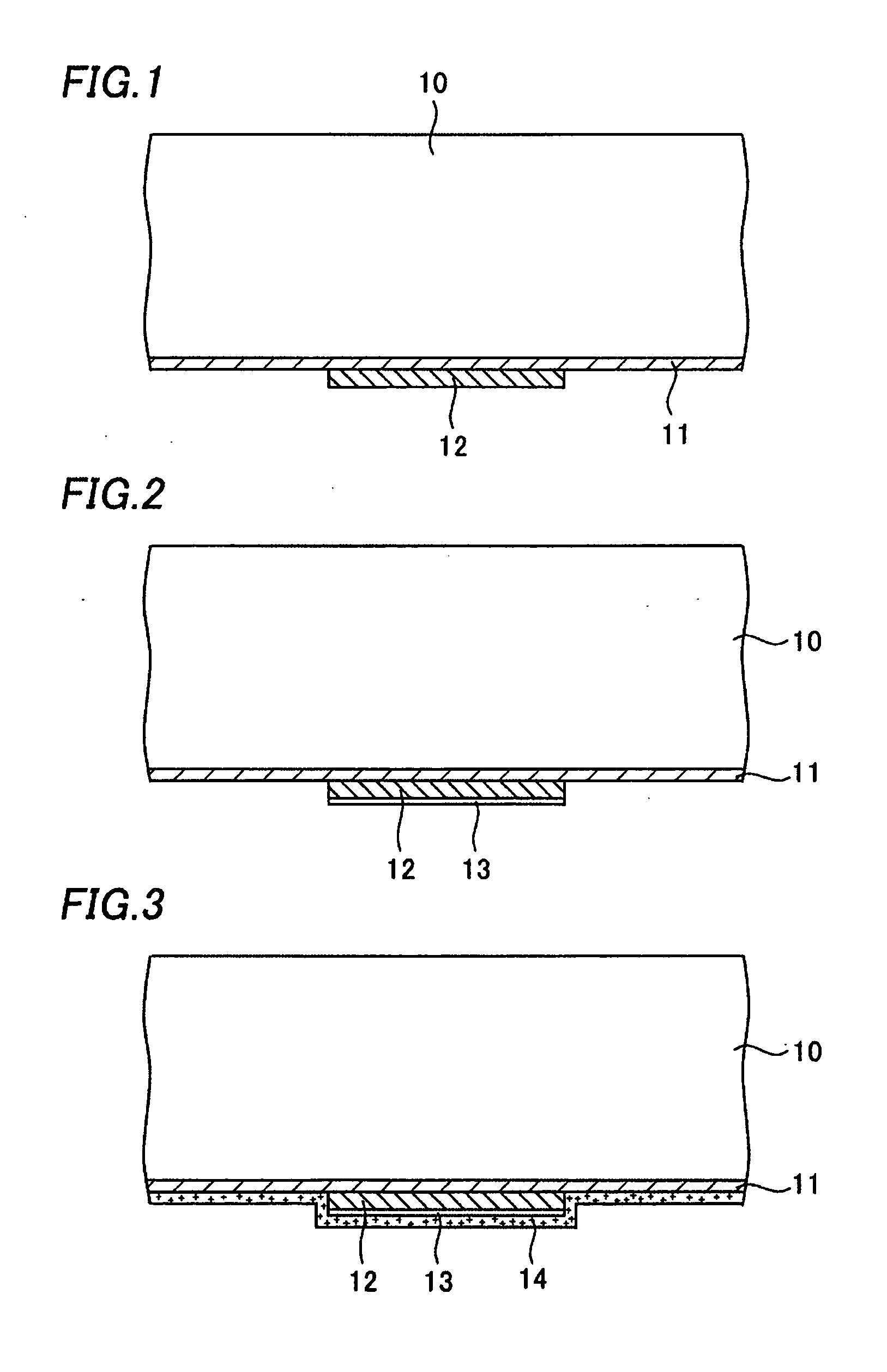
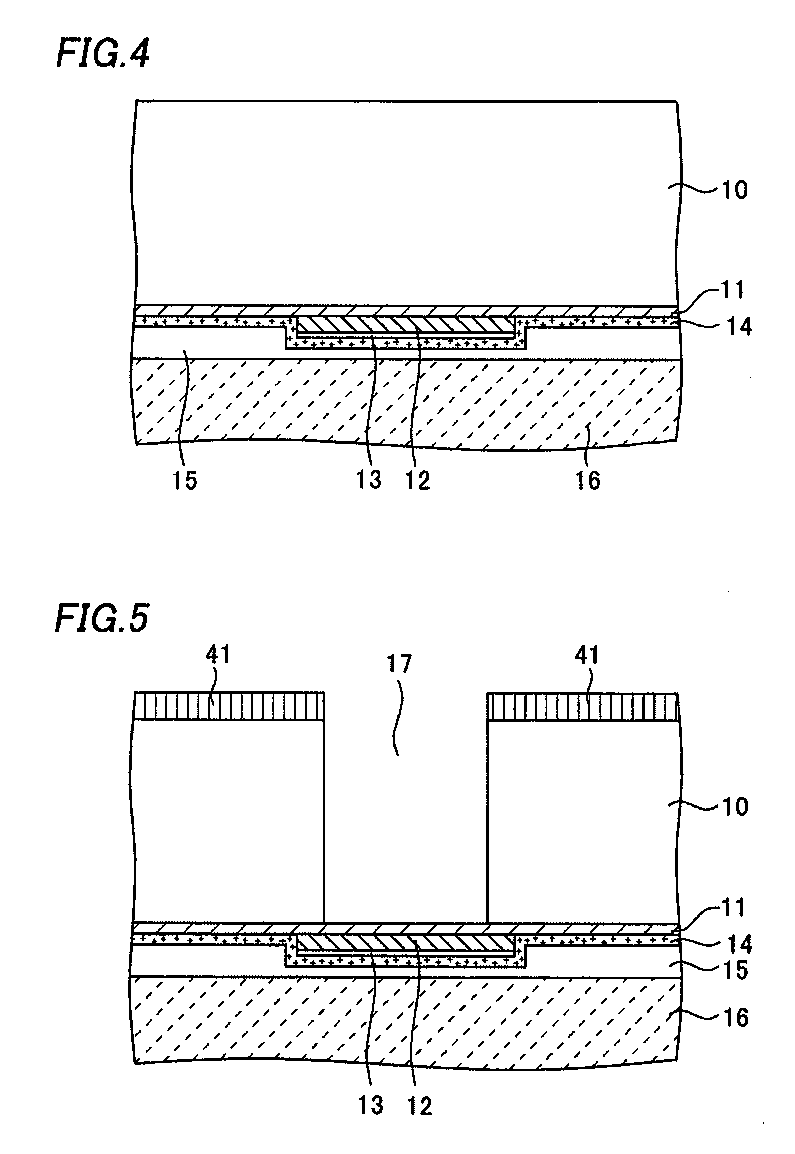
[0025] A semiconductor device manufacturing method of an embodiment of the invention will be described with reference to figures. FIGS. 1 to 13 are cross-sectional views showing the semiconductor device manufacturing method of the embodiment. FIGS. 1 to 13 show a portion of a semiconductor substrate near a dicing line (not shown).

[0026] First, as shown in FIG. 1, a semiconductor substrate 10 formed with an electronic device (not shown) on its front surface is prepared. The electronic device (not shown) is a light receiving element such as a CCD (Charge Coupled Device) or an infrared ray sensor, or a light emissive element, for example. Alternatively, the electronic device (not shown) can be the other electronic device than the light receiving element or the light emissive element. The semiconductor substrate 10 is formed of a silicon substrate, for example, but can be a substrate formed of the other material. The semiconductor substrate 10 preferably has a thickness of about 130 μm...


PUM


Abstract

The invention is directed to a semiconductor device having a penetrating electrode and a manufacturing method thereof in which reliability and a yield of the semiconductor device are enhanced. A refractory metal layer is formed on a pad electrode formed on a semiconductor substrate with a first insulation film therebetween. Next, a passivation layer is formed on a front surface of the semiconductor substrate including on the pad electrode and on the refractory metal layer, and a supporting body is further formed with a resin layer therebetween. Next the semiconductor substrate is etched to form a via hole from a back surface of the semiconductor substrate to the pad electrode. Next, a penetrating electrode electrically connected with the pad electrode exposed at a bottom of the via hole and a wiring layer 21 are formed with a second insulation film therebetween. Furthermore, a solder resist layer and a conductive terminal are formed. Finally, the semiconductor substrate is cut and separated into semiconductor dies by dicing.

Description

CROSS-REFERENCE OF THE INVENTION [0001] This invention is based on Japanese Patent Applications Nos. 2004-310725 and 2004-313734, the content of which is incorporated by reference in its entirety. BACKGROUND OF THE INVENTION [0002] 1. Field of the Invention [0003] The invention relates to a semiconductor device and a manufacturing method thereof, particularly, a semiconductor device having a penetrating electrode and a manufacturing method thereof. [0004] 2. Description of the Related Art [0005] CSP (Chip Size Package) has received attention in recent years as a three-dimensional mounting technology as well as a new packaging technology. The CSP means a small package having almost the same outside dimensions as those of a semiconductor die packaged in it. [0006] Conventionally, BGA (Ball Grid Array) type semiconductor devices having penetrating electrodes have been known as a kind of CSP. This BGA type semiconductor device has a penetrating electrode penetrating a semiconductor subs...

Claims


Application Information

Patent Timeline
IPC IPC(8): H01L23/48
CPCH01L21/6835H01L21/76898H01L24/13H01L23/3114H01L23/481H01L24/10H01L2224/13099H01L2224/16H01L2924/01013H01L2924/01015H01L2924/01022H01L2924/01029H01L2924/01033H01L2924/01073H01L2924/01074H01L2924/01078H01L2924/01082H01L2924/04941H01L2924/04953H01L2924/01006H01L2924/014H01L2224/02371H01L2224/13022H01L2224/13024H01L2224/0401H01L2924/00H01L24/03H01L24/05H01L2224/02372H01L2224/0392H01L2224/05124H01L2224/05166H01L2224/05181H01L2224/05548H01L2224/05624H01L2224/05647H01L2224/13H01L2924/351H01L2924/00014H01L2924/013H01L23/055
Inventor KAMEYAMA, KOJIROSUZUKI, AKIRAUMEMOTO, MITSUO
Owner SEMICON COMPONENTS IND LLC
Why Eureka
Try Eureka