Method for growing nitride-based semiconductor with high quality

Active Publication Date: 2016-03-31
GWANGJU INST OF SCI & TECH
View PDF0 Cites 4 Cited by
  • Summary
  • Abstract
  • Description
  • Claims
  • Application Information

AI Technical Summary

Benefits of technology

[0013]According to an exemplary embodiment of the present disclosure, threading dislocations due to lattice mismatch at the interface between a substrate and a nitr

Problems solved by technology

Dislocations due to such lattice mismatch are transferred into the GaN thin film, so that the performance of an electronic device such as an LED and a solar cell is significantly degraded.
However, there is a problem in that the process of growing crystal is divided into two steps, which increases chances of processing failure caused by contamination, etc.
However, it fails to improve the basic cause of the defect density.
Accordingly, there is still a pro

Method used


Image

  • Method for growing nitride-based semiconductor with high quality
  • Method for growing nitride-based semiconductor with high quality
  • Method for growing nitride-based semiconductor with high quality

Examples


Example

BEST MODE

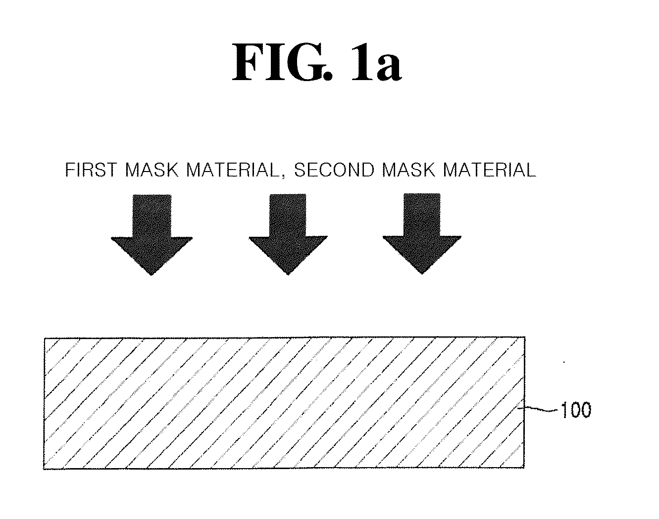
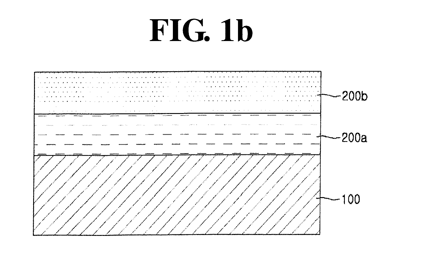
[0020]Hereinafter, exemplary embodiments of the present disclosure will be described in detail with reference to the accompanying drawings so as to enable those skilled in the art to easily practice the exemplary embodiments. However, exemplary embodiments of the present disclosure may be modified in various different ways and are not limited to those illustrated herein. In the accompanying drawings, non-essential elements are omitted in order not to unnecessarily obscure the gist of the present disclosure. Further, like reference numerals are used to denote like elements throughout the specification.

[0021]As used herein, a phrase “an element A on an element B” refers to that the element A may be disposed directly on the element B and / or the element A may be disposed indirectly on the element B via another element C.

[0022]Throughout the detailed descriptions, the terms “comprising” and “including” should not be interpreted as being restricted to the means listed thereafter;...


PUM


Abstract

Disclosed is a method for growing a nitride-based semiconductor with high quality, the method including: forming a first mask layer on a substrate and forming a second mask layer on the first mask layer; performing dry etching on the first mask layer and the second mask layer to form an opening in which a part of the substrate is exposed; performing selective wet etching on the first mask layer in the opening to form a recess in which a part of the substrate is exposed; depositing a third mask layer in the recess; and growing a nitride-based semiconductor from the exposed part of the substrate on sides of the third mask layer and expanding the growth via the opening.

Description

CROSS-REFERENCE TO RELATED APPLICATIONS[0001]This application claims the benefit of Korean Patent Application No. 10-2014-0128804, filed on Sep. 26, 2014, entitled “METHOD FOR GROWING NITRIDE-BASED SEMICONDUCTOR WITH HIGH QUALITY”, which is hereby incorporated by reference in its entirety into this application.TECHNICAL FIELD[0002]The present disclosure relates to a method for growing a nitride-based semiconductor with high quality. More specifically, the present disclosure relates to a method for growing a nitride-based semiconductor with high quality, by which threading dislocation defects are drastically reduced.BACKGROUND ART[0003]In manufacturing an electronic device by using the technology of growing a GaN film on a substrate such as sapphire, lattice mismatch due to the different lattice constants appears seriously at the interface between the substrate and the GaN film (see FIG. 5a). Dislocations due to such lattice mismatch are transferred into the GaN thin film, so that th...

Claims


Application Information

Patent Timeline
IPC IPC(8): H01L21/02H01L21/033H01L21/311
CPCH01L21/02639H01L21/0337H01L21/0332H01L21/31116H01L21/0254H01L21/31111H01L21/02642H01L21/02647H01L21/0331H01L21/30617
Inventor LEE, DONG-SEONSEO, DONG-JULEE, JUN-YOUBKANG, CHANG-MOSEONG, WON-SEOKPARK, MUN-DO
Owner GWANGJU INST OF SCI & TECH
Why Eureka
Try Eureka